Radio frequency (RF) and microwave amplifiers are designed to deliver optimal performance under specific bias conditions. The quiescent current, determined by the bias point, directly influences key performance metrics such as linearity, efficiency, and signal distortion. While some amplifiers feature internal biasing mechanisms, many require external power supplies to ensure proper operation. These external power supplies must be carefully timed to prevent damage and ensure safe and stable device performance.
Next, we'll focus on the importance of bias timing control in external bias amplifiers.
**Power Sequencing**
Proper power sequencing is crucial when using externally biased amplifiers for several reasons:
1. Improper power sequencing can lead to instability and even immediate failure if the breakdown voltage is exceeded. Repeated exposure to boundary conditions can reduce long-term reliability, and continuous violations of timing protocols may damage internal protection circuits, leading to field failures.
2. Optimizing bias levels during both power-up/power-down and normal operation can significantly enhance RF amplifier performance. This flexibility allows for dynamic adjustments based on application needs. For example, in adverse weather conditions like rain, output power can be increased to expand coverage, while in clear conditions, it can be reduced to save energy. External gate voltage control enables these adaptive features.
ADI offers a wide range of RF amplifiers, many of which are based on depletion-mode high electron mobility transistor (pHEMT) technology. These transistors typically require separate power supplies for the drain and gate pins, with the quiescent drain current depending on the gate voltage.
Refer to Figure 1 for the typical IV characteristics of a field-effect transistor (FET).
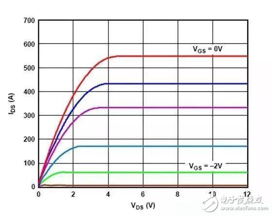
**Figure 1. Typical IV characteristics of a typical FET process**
As the gate-to-source voltage (VGS) increases, more electrons are attracted into the channel, resulting in a higher drain-source current (IDS). Similarly, increasing the drain-source voltage (VDS) enhances the electric field pulling electrons through the channel, further increasing IDS—especially in the linear region.
In practical RF amplifier designs, devices are often categorized into two types: self-biased and externally biased, due to factors like channel length modulation.
**Self-Biased Amplifiers**
Self-biased amplifiers include internal circuitry that sets the optimal bias point for operation. They are commonly used in broadband, low-power applications. Figure 2 shows a typical pinout for a self-biased amplifier.
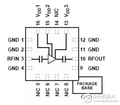
**Figure 2. Typical pinout of a multistage self-biased amplifier with multiple bias pins**
Although self-biased amplifiers are easy to use, they may not always deliver the best performance, as internal resistive biasing may not fully compensate for variations between batches, devices, or temperature changes.
**External Bias Amplifiers**
External bias amplifiers often provide superior performance under specific bias conditions. The quiescent drain current affects critical parameters such as power compression point, gain, noise figure, intermodulation distortion, and efficiency. For these high-performance devices, correct power sequencing is essential to ensure safe and reliable operation at peak performance.
Figure 3 illustrates a typical connection of an external bias amplifier's pins and their corresponding transistor connections. The diagram is a simplified schematic of the amplifier.
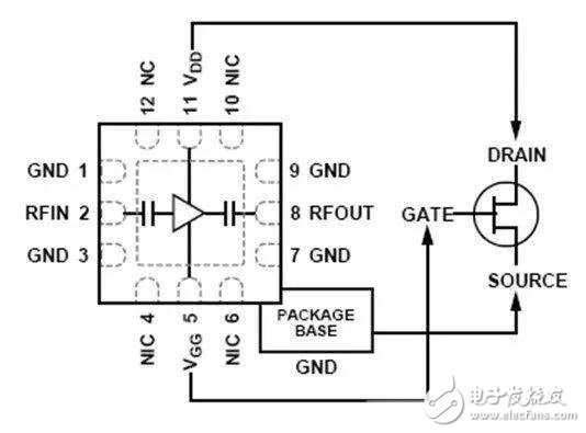
**Figure 3. Typical connection of an external bias amplifier**
Many external bias amplifiers are designed with multiple stages to meet various gain, bandwidth, and power requirements. Figure 4 shows the block diagram of the HMC1131, a multi-stage external bias amplifier.
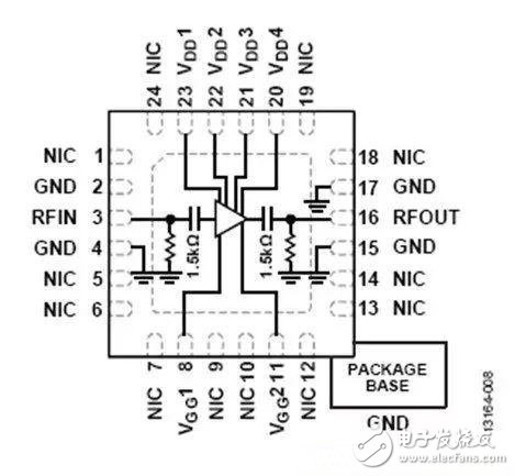
**Figure 4. HMC1131 Multistage External Bias Amplifier**
**Example: Timing and Control Requirements for an External Bias Amplifier**
The HMC1131 is a GaAs pHEMT monolithic microwave integrated circuit (MMIC) power amplifier operating from 24 GHz to 35 GHz. It delivers 22 dB gain, 23 dBm P1dB output power, and 27 dBm saturated output power. The recommended bias conditions are VDD = 5 V and IDQ = 225 mA. These specifications are listed in the HMC1131 datasheet for the 24–27 GHz frequency range.
To achieve a target IDQ of 225 mA, the gate bias voltages (VGG1 and VGG2) should be set between 0 V and -2 V. To avoid damaging the amplifier, follow the recommended power-up and power-down sequence.
**Recommended Power-Up Sequence for HMC1131:**
- Connect VGG1 and VGG2 to ground to set them at -2 V.
- Apply 5 V to the drain voltage bias pins (VDD1 to VDD4).
- Gradually increase VGG1 and VGG2 to reach an IDQ of 225 mA.
- Apply the RF signal.
**Recommended Power-Down Sequence for HMC1131:**
- Turn off the RF signal.
- Lower VGG1 and VGG2 to -2 V to bring IDQ close to 0 mA.
- Reduce VDD1 to VDD4 to 0 V.
- Increase VGG1 and VGG2 to 0 V.
When the gate voltage (VGGx) is at -2 V, the transistor is in the pinch-off region, and the quiescent current (IDQ) is nearly zero. Proper sequencing ensures the amplifier operates safely and efficiently under all conditions.
MINI FAKRA Automotive Cable Assembly
Dongguan Zhuoyuexin Automotive Electronics Co.,Ltd , https://www.zyx-fakra.com