Advanced Driver Assistance Systems (ADAS) is the fastest growing automotive application. According to market research firm Gartner, the market will grow from $5.6 billion in 2014 to $10.2 billion in 2018, achieving a 17.1% compound annual growth rate (CAGR) between 2013 and 2018; ADAS-related semiconductors Product consumption will grow from $1.38 billion to $2.4 billion at the same time, during which the compound annual growth rate will reach 15.5%.
Safety-oriented driving assistance system that supports pedestrian detection/avoidance, lane departure warning/correction, traffic sign recognition, panoramic imagery, fatigue monitoring, etc. These applications and many other applications (as shown in Figure 1) require A new class of system-on-a-chip (SoC) to meet the growing needs of the system.
With the help of consumer interests and government regulations, in order to improve road safety, automakers are asking Tier 1 suppliers (TIer 1) and semiconductor product suppliers to develop and incorporate the latest multimedia standards. A vision-based algorithm that combines the SoC of image and radar system sensor data.
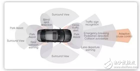
Figure 1 Various ADAS applications.
To achieve the advanced communication protocols required for high-performance operation, the ADAS SoC uses cutting-edge design and process technology that is more rigorous than most high-end consumer applications; designers of such components rely on IP vendors to help them overcome specific applications. The challenge of IP demand meets the demand for robustness, reliability and safety of automotive applications in a shorter design and forming cycle.
ADAS SoC Design Guidelines
From the two perspectives of applications and systems, these new ADAS SoCs have specific design guidelines to ensure efficient SoC design implementation; designers building SoCs for ADAS applications need to combine high performance and power saving IP Features to assist in achieving overall system throughput and meeting real-time quality of service requirements (Figure 2).
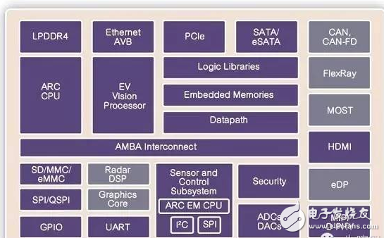
Figure 2 uses the 16/14 nm process ADASSoC, the purple part of which is Synopsys' Design WareIP product.
The performance requirements of such application processors are at least 32-bit, 1 GHz or higher-frequency processors; in fact, ADAS SoCs that support multiple vision-based applications have begun to shift to 64-bit. In addition to high-performance application processors, such SoCs require a separate vision processor to implement the latest visual algorithms such as ConvoluTIonal Neural Networks (CNN).
In addition, an additional graphics processor or custom digital signal processor (DSP) core is responsible for high-rate pixel processing and links to multimedia interfaces such as High Definition Multimedia Interface (HDMI) or Mobile Industry Processor Interface (MIPI) D-PHY. At the same time, it supports high-definition displays with ever-larger sizes. To support multiple cameras and radar sensors that provide imaging and radar/lidar data, a sensor and control subsystem is needed to share sensor data management tasks for the application processor (ApplicaTIon Processor) to achieve high-level sensors. Fusion.
The new generation of ADAS SoCs requires up to 8GB of LPDDR4 memory to support processor applications, and Ethernet AVB and TIME Sensitive Networking (TSN) to provide a wide range of systems for supporting multimedia data traffic. link. The SoC peripheral provides additional interfaces such as PCI Express, SATA, Universal Asynchronous Receiver Transmitter (UART), SPI/QSPI, CAN and FlexRay.
Finally, in order to support cloud links implemented by external Bluetooth Smart, Wi-Fi or 4G LTE wireless chips, the ADAS SoC must include a robust, hardware-based secure communication protocol to support secure boot, secure identification and Identity verification, encryption, and decryption.
In addition to the IP capabilities that ADAS SoC design engineers must consider, automotive industry Tier 1 component suppliers and semiconductor SoC designers and architects also need to consider latency, power, reliability, and process-related design challenges.
Low latency is a fundamental principle in response to real-time multimedia service level assurance; in addition to low latency, such SoCs are constantly adopting the latest multimedia protocols and key features such as embedded visual processing capabilities required for specific ADAS applications such as pedestrian detection and correction. At the same time, you need to maintain the lowest power consumption. Another key challenge for ADAS SoC designers is to ensure the high reliability and continuous operation required by the OEM, so the chip needs to implement critical error checking and correction (ECC) and equivalent technology.
Due to the need for high performance and high integration, designers are locking in advanced semiconductor processes such as the 16/14 nanofin field effect transistor (FinFET) process node that many design teams are not yet familiar with. For the next-generation automotive ADAS application SoC, SoC challenges such as low latency, low power consumption, advanced communication protocols, ECC, and the availability of mission-critical IP in the 16/14 nm FinFET process are key issues.
The FirstPower CFPV(2V) and LFPV(6V/12V) series stationary batteries (OPzV battery) are the newly products which were developed at the end of 2005.
The performances meet the standard DIN40742 and IEC60896 TubularPositive plate, gel electrolyte, PVC-SiO2 and redundant design makes the battery the most reliable battery. The design life is more than 20 years.
Industrial Opzv Battery,Maintenance Free Opzv Industrial Battery,Opzv Battery Industrial Stationary Batteries
Firstpower Tech. Co., Ltd. , https://www.firstpowersales.com