Deep interference analysis of common-impedance interference of ground interference (pcb board design must know)
Common Ground Interference
1. The Starting Point of This Article
Based on the principles of noise generation, this article further explores practical and simple applications—specifically, the most straightforward method to avoid noise in digital-analog hybrid audio systems: "single-point grounding." The goal is to help readers understand why it's important to ground at a single point. It's hoped that readers will focus on the underlying principle of single-point grounding, so they can apply and extend this knowledge beyond the examples provided here, rather than just memorizing them.
2. Target Readers of This Article
Does the term “single-point grounding†sound familiar?
If you're currently thinking, “I've heard about single-point grounding, but I don’t know how to implement it; or I know how to do it, but I’m not clear on the underlying theory,†then you're in the right place! This article is written specifically for you.
3. Common Forms of Resistance Interference
This paper focuses on several common forms of resistance interference, which can lead to classic consequences such as noise amplification, signal attenuation, noise reduction, and local interference output.
The root cause of common resistance interference is: the ground wire has impedance, and the interfering signal shares a common loop with the signal being interfered with.
3.1. Several Forms of Common Resistance Interference
3.1.1. No Common Resistance Noise
Ideally, the wire has no impedance, no distributed parameters, and no noise. Av-noise = 0:
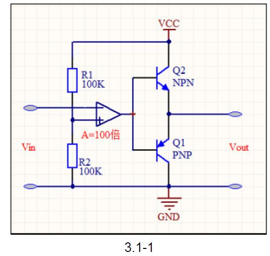
As shown in Figure 3.1-1, ideally, Vout = 100*Vin, and there is no noise in the output.
3.1.2. Worst Case of Common Resistance Noise
In the worst case, the noise is "doubled." Av-noise >> 1:
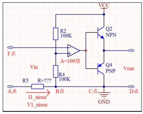
Figure 3.1-2
As shown in Figure 3.1-2, the AB segment is a piece of copper foil on the PCB, which inherently has some impedance (even though the resistivity of copper is very low). Assuming its impedance is R5. The analog input signal passes through the A-B segment. When the digital current I1-noise loops through the A-B point, R5 becomes both the return path for the analog signal and the return path for the digital circuit. This shared return path is called "common resistance." The digital signal generates V1-noise after R5, which is superimposed on the clean analog input signal, causing contamination (interference). This type of interference is known as "common resistance interference."
Since the circuit amplifies the voltage at the BF terminal (not just the AF side), Vout = (Vin + V1-noise) * 100. Thus, the noise is amplified by 100 times! This is the most severe case of common resistance interference.
Empirical interpretation: Some people argue that since the resistivity of copper is so low, even if V1-noise is amplified by 100 times, it's still not audible, because the oscilloscope shows no noise at all. However, this argument seems logical but isn't entirely accurate. First, the human ear can detect millivolt-level noise in a quiet environment through headphones, while ordinary oscilloscopes may not capture such weak signals. Second, even if the digital circuit operates above 20kHz, the switching between internal modules might fall within the audible range. Additionally, even high-frequency digital signals can be filtered by wire inductance and capacitance, resulting in audible noise.
3.1.3. Common Resistance Noise 1:1 Amplification Output
The interference is not amplified and appears directly at the output. Av-noise = 1:
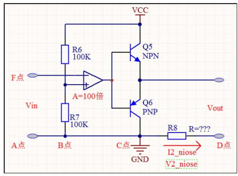
Figure 3.1-3
As shown, when only digital noise flows through R8, Vout = Vin * 100 + V2-noise. There is digital noise, but it’s not amplified, so it’s usually not noticeable under normal conditions. However, it may become audible in a quiet environment.
3.1.4. Common Resistance Interference Is Attenuated and Output
The interference is suppressed by the power amplifier device. Av-noise << 1:
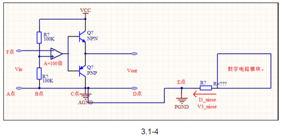
As shown in the figure, if the digital circuit is grounded at a single point, the digital noise V3-noise can return directly to the power supply without passing through the power amplifier area. Although there is still a small amount of noise flowing through the EC segment of the PCB, the effect is minimal. The reason is that the noise is returned via the power supply, not the ground line. However, two things should be considered:
(1) The power supply is not ideal and has internal resistance. Therefore, the digital circuit can interfere with the power amplifier by affecting the common power supply. Fortunately, this interference is very small, and the power amplifier typically has high ripple rejection capability.
(2) C and E are also copper foil with internal resistance. This ground line can cause common resistance interference. However, in practice, this doesn’t cause issues because the interference is equivalent to power supply jitter, and the power amplifier has some power supply ripple suppression capability. Some chips have better power ripple suppression than ground ripple suppression, related to the bypass circuit. Interested readers can explore further.
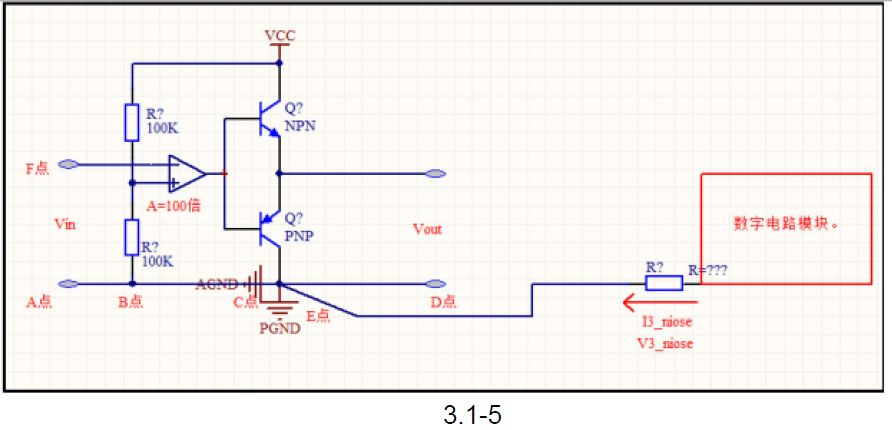
3.1.5. No Ground Noise on the Circuit Board
As shown in Figure 3.1-5, the single-point grounding of the battery, digital ground, and analog ground is connected at points C and E. This configuration ensures no noise on the board, Av-noise = 0.
(However, after the battery is connected, a similar situation to 3.1.4 occurs, because each power supply has internal resistance. Readers are encouraged to analyze this model themselves!)
3.2. Sensitive and Insensitive Points
Understanding the content of Section 3, proper PCB trace layout can result in noise being "multiplied" or "1x amplified." This section explains that in audio amplifier circuits, there are "ground noise sensitive and insensitive segments" on the PCB.
3.2.1. Ground Noise Sensitive Segment PCB
The AB segment in Figure 3.1-2 is a sensitive PCB segment because the noise passing through it is amplified. Digital ground noise through this segment will be "doubly amplified" and output.
The reason for this doubling is that the noise signal passes through the front-end amplifier's ground return path. This PCB corresponds to the "capacitor grounding point" and the power ground of many power amplifiers. In other words, the PCB between BC is likely to become a ground noise sensitive segment.
3.2.2. Ground Noise Insensitive Segment PCB
The CD segment in Figure 3.1-3 is an insensitive PCB segment, as the noise amplification factor is 1, and the noise won't be doubled. The reason is that the ground noise does not pass through the preamplifier area of the power amplifier, so the noise is only output locally at the speaker end.
4. Single-Point Grounding
The main idea of this section is that in various cases of common resistance interference discussed in Section 3, ground noise may flow through the "sensitive PCB segment." To minimize ground noise, single-point grounding is required to prevent noise from passing through these sensitive areas.
4.1. Connection Between Single-Point Grounding and "Sensitive Signal Segment"
Careful readers may have noticed that single-point grounding is already mentioned in Section 3. Single-point grounding should not be understood as merely having a physical grounding point on the PCB. Instead, it means that different ground return signals (like analog and digital) do not share a common path outside the grounding point (common path – i.e., the ground resistance shared by digital and analog signals).
Figures 3.1.4 and 3.1.5 actually represent single-point grounding, so there is no need to repeat them here. This section focuses on how to truly understand and apply single-point grounding.
4.2. How to Understand Single-Point Grounding
The concept of single-point grounding is thoroughly explained in the book "Printed Circuit Board Layout Design." Although the design techniques may differ slightly from today, the core idea remains the same. The author believes this is one of the few Chinese books that avoids copy-pasting. Thanks to Zheng Lao for his work!
4.2.1. Importance of Understanding the Principle (Experience Nonsense)
We often hear the term "single-point grounding." Many say that it's the ultimate solution to eliminate noise in digital-analog hybrid circuits. But one day, someone comes rushing over and says, "I’ve grounded at a single point, but the noise is still there..." Why? Because "correct" single-point grounding is needed, not just any single point. The correct grounding point for digital, analog, and power grounds is usually the power ground pin of the power amplifier or the decoupling capacitor pin.
When designing real products, there are many wiring rules that can't be followed simultaneously. Deciding which rule to follow requires understanding what's most impactful and what's negligible. Hence, theory is essential alongside practice.
4.2.2. Example: Understanding Sensitive Signal Areas
Before using a chip, it's important to evaluate its characteristics. This requires theoretical and professional knowledge to infer its internal structure and determine which parts are sensitive and which are not.
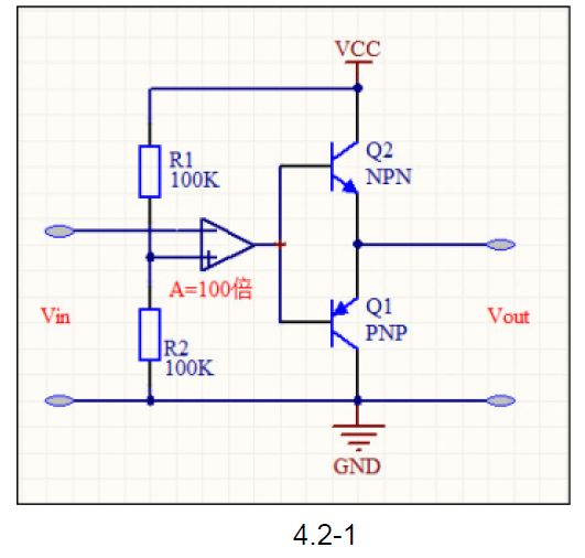
For example, in most AB audio amplifiers, the front end is a voltage amplifier, equivalent to an op-amp, composed of a bias circuit and a common-emitter amplifier. Its function is to amplify the input signal, including noise. The latter stage is an emitter follower, with a voltage gain of 1 but higher current driving capability.
The "+" terminal of the op-amp is usually equivalent to the bypass pin of the amplifier, and the ground of Q1 is equivalent to the power ground pin. The bypass pin is usually connected to a decoupling capacitor to ground. The PCB trace of the capacitor ground to the amplifier’s power ground is equivalent to the AC segment in Figure 3.1-2. If there is noise in this PCB, it will mix into the op-amp in the preamplifier stage, leading to significant noise amplification.
This is referred to as "noise mixing into the sensitive signal PCB segment." Therefore, the purpose of single-point grounding is to prevent noise from returning through the "ground area of the sensitive signal segment."
5. Extension of Theory
This section draws a single-point power supply from single-point grounding and discusses the "power supply ripple rejection ratio" based on the phenomenon that single-point power supply is "not universally sufficient." It proves in principle that analog chips have strong power supply ripple suppression, while digital chips do not.
5.1. Since There Is a Single-Point Grounding, Is There a "Single-Point Power Supply"?
Yes, of course. But why do predecessors emphasize "single-point grounding" more than "single-point power supply"? It’s similar to life: things that happen frequently or have serious consequences are often remembered, while rare or minor ones are ignored.
Similarly, "single-point power supply" is less emphasized. While power supplies can generate common-resistance noise, in audio amplifiers, the effect is usually small due to high ripple rejection. The power supply's common-resistance interference doesn’t appear as amplified noise, and thus is often overlooked in the audio field (especially for integrated chips). For discrete component power amplifiers, however, power supply ripple can be more critical.
5.2. Discussion on "Power Supply Ripple Rejection"
5.2.1. Overview: Sensitivity to Power Supply Ripple
Analog and digital circuits generally have different performances in suppressing "power ripple noise." Analog devices are typically not sensitive to power supply ripple and do not react significantly to it. Digital circuits, on the other hand, often reflect power supply ripple directly on the output.
Note: Analog circuits are sensitive to signal noise. Even small amounts of noise can affect the output. Digital circuits are relatively insensitive to signal noise, as they can still correctly interpret high and low levels even with large noise.
5.2.2. Reasons for Strong Ripple Suppression in Analog Circuits
General amplifiers and op-amps process analog signals. They can amplify or reduce signals by a factor of N and usually have strong power supply ripple (noise) suppression capabilities. At least, the noise on the power supply is attenuated by more than 10,000 times.
Why do analog devices like op-amps have such strong power supply rejection? It's due to regulated power supplies, constant current sources, and non-saturated amplifier circuits used in their internal structures. These circuits provide strong power supply ripple suppression.
A deeper analysis is beyond the scope of this article, but a basic circuit model inside the chip can be briefly described. Why does the common-emitter amplifier have strong power supply ripple suppression?
PS: Readers interested in in-depth research can refer to "Basics of Analog Electronic Technology" (Children's White Edition 4) and related topics for further study.
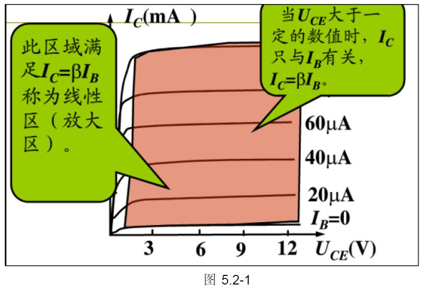
This figure is a classic "triode characteristic curve," which already contains the message that the common-emitter amplification area has strong power supply ripple suppression capability!
Really? No way? — Please see the analysis.
I lied to you earlier. — Please read the explanation carefully.
For a common-emitter amplifier circuit, suppose in the amplification area (the brownish red region in the figure), the transistor B provides a fixed electrode current Ib1 = 20uA. Even if the power supply voltage (Uce) fluctuates between 3V and 9V, Ic1 remains essentially unchanged (as seen in the figure). Ic1 remains unchanged, meaning the output voltage of the common-emitter amplifier is also unchanged! (To understand this sentence, you must grasp the basics of the common-emitter amplifier circuit.)
Therefore, for the triode common-emitter amplifier in the figure, if a Vin signal is input at the B-terminal, even if the voltage fluctuates between 3V and 9V, the output is only related to the input, and is basically unaffected by the power supply voltage fluctuations. This shows that this amplifier has strong power supply rejection.
5.2.3. Digital Circuits Have No Power Ripple Suppression Capability
Low-power three-stage tubes have a very small drop in saturation conduction when the output current is not very large, and can be considered zero. (Many hardware engineers question this pressure drop. Then, use data to verify. Oh! So when the input is 3.3V, the output is 3.3V.)
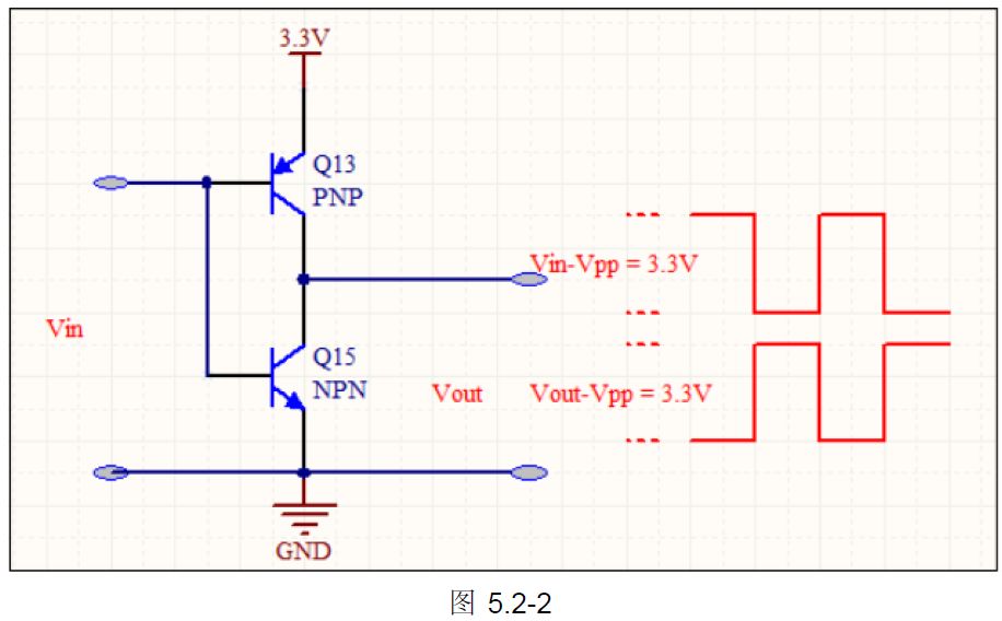
When the supply voltage changes from 3.3V to 10V, all digital circuits operate at 10V, and the voltage of each digital gate is also 10V. So the result is: Vin and Vout are the same—both are 10V.
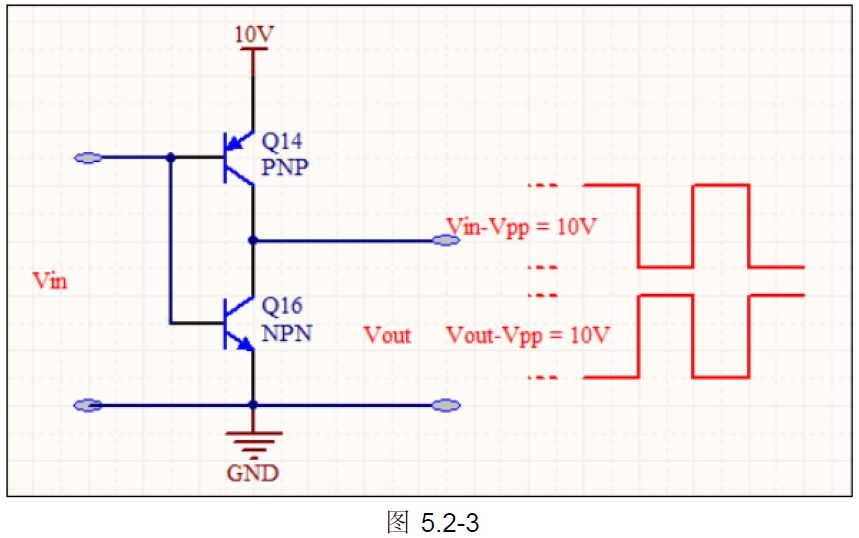
Thus, since the IO port of the digital circuit operates in saturated conduction (which cannot be discussed in special ECL circuits), the output voltage is always equal to the power supply voltage. Therefore, power supply fluctuations are reflected unreservedly on the output, resulting in zero power supply ripple rejection. This characteristic is crucial in handling digital circuit mutual interference.
6. The Essence of This Article
(1) The interference caused by the common return path is called "common resistance interference."
(2) The human ear can clearly detect millivolt-level audible noise through headphones in a quiet environment, while ordinary oscilloscopes generally cannot capture such weak waveforms.
(3) Because common resistance interference affects the "sensitive PCB segment" of the ground noise, it is necessary to perform single-point grounding to prevent noise from passing through the sensitive PCB segment.
(4) The concept of single-point grounding is detailed in "Printed Circuit Board Layout Design." (Author: Zheng Wei Poem)
(5) Generally, analog devices are insensitive to power supply ripple and do not significantly react to it, while digital circuits typically reflect power supply ripple on the output.
Usb Otg Adapters,Usb4 Female To Type-C Male Otg Adapter,Customizable Thunderbolt Otg Adapter Cable,Usb3.2 Female To Usb-C Male Otg Adapter
Dongguan Pinji Electronic Technology Limited , https://www.iquaxusb4cable.com