Voltage is one of the most basic measurement elements in electronic and power systems. Fast and accurate voltage acquisition has always been one of the important contents of data acquisition and electronic measurement instruments. The traditional pointer voltmeter has the defects of low precision, close visual distance and single function, which is not suitable for the development of high-speed informationization. At present, the digital voltmeter widely used on the market has a low degree of intelligence. When measuring voltage, it is necessary to manually switch the range. If the range selection is not correct, the measurement accuracy will drop, and even the extreme situation of the voltmeter will be burned out. Digital voltmeters generally use complex circuits such as DSP, FPGA or CPLD, and the hardware and software implementation costs are high. To this end, the author designed and developed a smart AC DC voltage data acquisition system with single-chip microcomputer as the main control body, which has the advantages of small size, high precision, simple structure, convenient use and reading, high cost performance and wide adaptability. Make up for the shortcomings and drawbacks of the above various voltmeter systems.
1 system overall plan
The voltage data acquisition system is mainly composed of voltage attenuator, range conversion and amplification circuit, AC/DC conversion circuit, A/D conversion circuit, main control single-chip STC89C52 and LCD display circuit. The principle block diagram is shown in Figure 1. Show. The voltage attenuator and the amplifier convert the analog signal voltage value to be tested into the input voltage range of the AC/DC converter, and the DC voltage is attenuated and amplified without AC/DC conversion; the range conversion circuit is based on the input to the A/D converter. The analog DC voltage is determined by the MCU, and the control relay adjusts the attenuation amplifier circuit accordingly to ensure that the optimal range is selected. The A/D conversion is initiated by the MCU, and the collected data is digitally filtered and scaled in the software. After processing such as transformation and system error calibration, the measured value and voltage type are displayed on the LCD according to the voltage type flag.
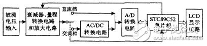
Figure 1 Block diagram of the voltage data acquisition system
2 system hardware design
2.1 Voltage attenuation, amplification and range conversion circuit
The voltage attenuation amplification and range conversion circuit is shown in Figure 2. The resistors R1 to R5 form a voltage divider with attenuation coefficients of 1, 10, 100, 1 000, and 10 000, respectively, and the measured input voltage Uin is attenuated to a range of 0 to 200 mV and sent to the back-end circuit for amplification, AC/DC. Conversion (DC voltage does not need to be converted), A/D conversion, and acquisition, processing and display by the microcontroller. In order to reduce the measurement error, the voltage dividing resistors R1 to R5 select precision metal film resistors with an error of ±0.5%. The range selection is controlled by the P1.0~P1.4 line of the MCU through the inverter 74HC04, which controls the input end 1 B~5 B of SPRAGUE's high withstand voltage and high current Darlington transistor integrated circuit ULN2003. The contact switches that drive the electromagnetic relays K1 to K5 are activated or closed. The AC voltage and the DC voltage share the same conversion range. When the K1 to K5 are independently connected, the corresponding ranges are 200 mV, 2V, 20 V, 200 V, and 1 000 V (AC 750 V). If the measured voltage is higher than the range set by the single-chip microcomputer, the single-chip microcomputer controls the corresponding relay coil to attenuate the signal, and vice versa, to ensure that the signals input to the AC/DC converter and the A/D converter do not exceed their values. Operating voltage range. Since the measured voltage is unknown, to avoid burnout of the circuit, the initial range should be set to the highest range.
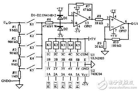
Figure 2 voltage attenuation amplification and range conversion circuit
ULN2003 chip internal diode negative common terminal COM is connected to the load power supply +5 V, which acts as a reverse freewheeling action for each relay coil. The purpose of adding the inverter 74HC04 is to prevent the input high voltage from directly entering the low-level weak current system without causing the partial voltage to cause the circuit to burn out when the single-chip microcomputer system is powered on or reset. The op amp U3 is connected in the form of a voltage follower, which functions as a channel before and after isolation, and reduces the output impedance and improves the load capacity. Among them, R6 and R7 are current limiting resistors to prevent excessive current caused by the range switching to each range; D1 and D2 are bidirectional limiting diodes, which provide overvoltage protection. The op amp A4 and the resistors R8, R9, and R10 are connected to the same analog circuit, and the signal attenuated in the range of 0 to 200 mV is amplified by 10 times and sent to the following AC/DC converter AD637J (nominal full scale is 2V) for AC/ DC conversion f DC does not need to be converted).
2.2 AC / DC conversion circuit
AC/DC converter circuit shown in Figure 3, two single-channel single-pole double-throw (SPDT) analog switch MAX14763 complete AC / DC voltage channel switching function, a high-performance true RMS TRMS (True Root MeanSquare) converter AD637K Complete AC and DC voltage conversion function.
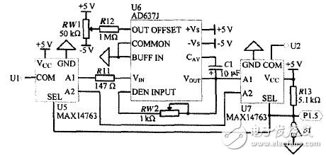
Figure 3 AC / DC conversion circuit diagram
The MAX14763 is a +3.0 V to +5.5 V single-supply device that allows bipolar signals to exceed ±25V beyond its supply voltage swing. The maximum on-resistance and on-lead leakage current are 2Q, ±100 nA, respectively. The lower on-resistance and wider frequency band (a 3 dB bandwidth is 1O0MHz) make it ideal for digital and analog signal switching applications. When the toggle switch S1 is closed, the SEL terminal of the MAX14763 is low, the C0M terminal is connected to A1, the AC voltage channel is connected, and the input AC voltage is AC/DC converted; otherwise, the DC voltage channel is turned on, and the DC input is enabled. The voltage goes directly to the downstream circuit.
The AD637K is a complete high precision, single-chip rms-to-dc converter that calculates the true rms TRMS of any complex input waveform without regard to waveform parameters and distortion, and provides equivalent DC The output voltage. which is:
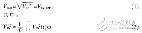
T is the measurement time and V IN(t) is the input signal waveform. It can be seen that the true rms value of the waveform is directly related to the signal power and therefore more useful than the average rectified signal. The accuracy of the AD637K is ± (0.25 mV + 0.05% RDG). Allows measurement of input signals with an effective value of 200 mV and frequencies up to 600 kHz and input signals with rms above 1 V and frequencies up to 8 MHz. The maximum full-scale range of the AD637K is 7 V. Since the rms 2V full-scale range provides a larger headroom for the peak input (high-peak factor signal), the attenuating amplifier output signal U1 should be controlled within this range. . The average capacitance C1 in the circuit is used to set the mean time and determine the low frequency accuracy, output ripple size and settling time. Potentiometers RW1 and RW2 are used to zero and amplitude the output, respectively, to make the output more accurate.
2.3 A / D conversion circuit
The A/D conversion circuit is shown in Fig. 4, in which the operational amplifier U8 and the resistors R14 to R16 constitute a non-inverting amplifying circuit, and the DC voltage of the front end output U2f ≤ 2 v) is doubled, and the measurement resolution of the input voltage Uin is improved. Doubled. The MAX187 is a serial 12-bit successive approximation A/D converter that operates from a single +5 V supply and contains an on-chip clock and sample/holder for sampling rates up to 75 kHz. It is connected to the I/O port line P2.0~P2.2 of the MCU through a high-speed 3-wire serial interface. The interface is compatible with SPI, QSPI and Microwire bus protocols. SHDN is connected to the high level, and the REF terminal is connected to the ground by 4.7 F. This is the internal 4.096 V reference voltage. The analog input signal at the AIN terminal is in the range of 0 to 4.096 V.
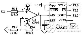
Figure 4 A / D conversion circuit diagram
2.4 LCD display circuit
The system uses the 5110 liquid crystal display (LCD) module produced by NOKIA as the display unit to complete the function of displaying the current voltage value and voltage type (AC or DC). The circuit is shown in Figure 5. The NOKIA 5110 has only 5 signal lines connected to the microcontroller, and the interface circuit is simple. Its communication protocol is an SPI protocol with no MISO and only MOSI. The transmission rate is up to 4 Mb/s, and the display data can be written at full speed without waiting time. It can be simulated by a single-chip software program. SPI is connected to 15 write data / command timing (transfer 1 B) as shown in Figure 6.
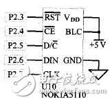
Figure 5 LCD display circuit diagram
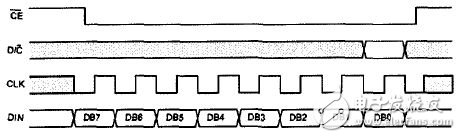
Figure 6 NOKIA5110 Serial Bus Protocol
3 system software design
3.1 System Software Overall Process
The overall flow chart of the system software is shown in Figure 7. In order to facilitate the porting, calling and debugging of the program, the modular programming idea is adopted to program the modules of different specific functions separately. The microcontroller is powered on to initialize the program, complete the hardware settings of the K1~K5 relay, MAX187 and NOKIA5110, as well as the initialization of the internal system interrupt and system variables of the microcontroller. Then select the highest range (set the PI.4~P1.0 line status to 011l1), start the A/D conversion test signal and perform data processing calculation, and judge whether the range is suitable. The overrange and underrange thresholds are taken as 4000 and 400, respectively, and the corresponding ADC input voltages are 4V and 0.4V, respectively. If the current range is appropriate, the measured digital value is obtained by scaling and error calibration of the processed digital quantity, and the voltage type, effective value and unit information are displayed on the LCD. Conversely, the range is switched to find a new optimal range, and the next measurement is performed under the newly selected range. In the judgment, if the range is still the under-range, the original range will not change; if the range is the highest, it will still be over-range, then the corresponding overload measures must be taken.
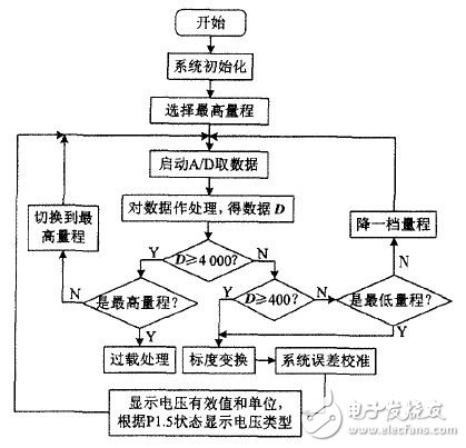
Figure 7 is the overall flow chart of the game software
3.2 Digital filtering of sampled data
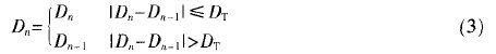
When processing the A/D sampled data, the program judgment filter method and the moving average filter method are used successively. The former is used to eliminate the spike interference signal caused by accidental factors such as random interference, false detection or system instability. It is used to suppress high-frequency interference caused by periodic interference components such as radio waves that may appear in the data. The program judgment filtering algorithm judges according to the practical experience to determine the maximum deviation value DT allowed by the adjacent sampling (here, the value is 8), and each time a new value is detected, it is judged: if the difference between the current value and the previous value is If the absolute value is less than or equal to DT, the current sample value is valid; instead, the current value is discarded, and the previous value is substituted for the current value. As shown below:
After the pulse interference is eliminated, the data is further processed by a moving average filtering algorithm. It treats consecutive N samples (here, N=10) as a queue of length N, puts a new value into the end of each queue, and throws away the data of the original leader, and then the N in the queue. Data is arithmetic averaged to obtain new filtering results 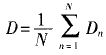 This data is used for threshold discrimination and scale conversion.
3.3 System error calibration algorithm
Due to the non-ideal characteristics of the system circuit's reference error, amplifier's zero drift and offset, gain error and nonlinearity, system errors are caused. In order to improve the measurement accuracy, the following algorithm is used for error calibration and compensation. Let the equal-precision measurement obtain the group voltage sample data (Xi, Yi), where: i = l,..., M, Xi, and Yi are the scaled voltage value (measured value) and the actual value respectively (by the high-precision voltage reference source) produce). Using the least squares method, the measured data is linearly fitted to Y=aX+b, based on the weighted sum of squared deviations of the sample data. 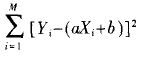 The minimum principle, the mathematical expressions of the coefficients a, b are as follows:
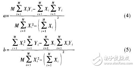
Substituting each correction point data (Xi, Yi) (where M is 6) into the above two equations to obtain the values ​​of coefficients a and b, and store them in the memory unit of the microcontroller. At the time of the formal measurement, the correction value Y is obtained from the measured value and the error correction equation Y = aX + b, thereby eliminating the systematic error. Since the system error is different due to different ranges, it is necessary to perform the above processing on each range to obtain the best calibration effect for different ranges.
4 main technical indicators
The main technical indicators of the system are as follows: (1) Range: 200 mV, 2 V, 20 V, 200 V, 1 000 V (AC 750 V); (2) Resolution: 50 txV, 0.5 mV, 5 mV, 50 mV, 0 .5V (corresponding to each range); (3) Accuracy: 200 mV: 0.005% & TImes; reading +0.0025% & TImes; fullness (DC), 0.05% & TImes; reading +0.05% &TImes; fullness (AC); other files: 0.005% × reading + 0.001% × fullness (DC), 0.05% X reading + 0.025% X fullness (AC); (4) Working power: DC ± 5V.
This paper designs and implements an AC/DC voltage data acquisition system based on single-chip microcomputer with automatic range conversion function. It has wide measurement dynamic range and provides a cost-effective solution for high-precision voltage data acquisition and intelligent voltmeter research. . The actual operation results show that the system has high precision, small error, high sensitivity, stable operation and reliable performance. It can be widely used in power system, metrology, defense industry, household appliances, technology and industrial production, railway equipment, etc. Get the various areas. In addition, some hardware and software design methods and ideas used in the design also provide reference for the design and development of similar data acquisition systems and intelligent instrumentation.
New ! ! !
New ! ! !,High Quality New ! ! !,New ! ! ! Details, CN
Wuxi Sunket New Energy Technology Co.,Ltd , https://www.sunketsolar.com