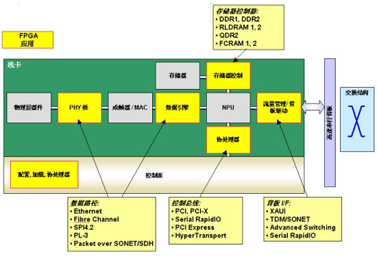
Figure 1: Application on the FPGA Online Card
LatticeSC FPGAs use Fujitsu's 90nm CMOS process technology and are fabricated on 300mm wafers, which accelerates chip-to-chip, chip-to-memory, high-speed serial, backplane, and network data channel connectivity. This article describes the features, structure, and applications of the LatticeSC FPGA. LatticeSC devices are designed for high-performance protocol-based connectivity architectures that support multiple protocols and all high-performance memory standards.
Device structure
The device integrates a high channel count SERDES module supporting 3.4Gbps data rates, PURESPEED parallel I/O with industry-leading 2Gbps speeds, an innovative clock management fabric, FPGA logic operating at 500MHz, dense RAM blocks, and Lattice has a masked array of cost-optimized (MACO) embedded structured ASIC modules. Figure 2 shows the structure of the device.
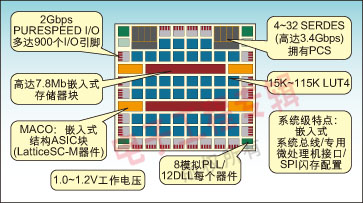
Figure 2: Structure of the device
Although structured ASICs lack the flexibility of FPGAs, they are becoming more and more popular due to their density and performance. Unlike fully custom or standard cell ASICs, structured ASICs are much less expensive to design because they use only a small portion of the mask for customization. Lattice has embedded up to 12 structured ASIC modules in each LatticeSC FPGA, called the MACO module. Approximately 50,000 ASIC gates per MACO module can be used to implement IP cores that require the highest performance, the smallest silicon area, and the lowest power consumption. The MACO module also provides sufficient wiring connections to I/O pins, RAM blocks, and programmable logic blocks.
The LatticeSC device offers 1- to 7.8-megabit embedded RAM block (EBR) capable of operating at 500MHz. Each 18Kb sysMEM EBR block can implement single-port, dual-port, pseudo-dual-port, or FIFO memory. The dedicated FIFO support logic enables the LatticeSC device to implement the FIFO efficiently without the need to use LUT or routing resources to generate the flag. The device also integrates a hierarchical clock resource. Unlike Other devices, LatticeSC FPGAs have both PLL and DLL resources, providing a "no compromise" solution to clock management issues.
In addition to SERDES, LatticeSC PURESPEED I/O supports many differential and single-ended I/O standards including LVTTL, LVCMOS, SSTL, HSTL, GTL+, LVDS, LVPECL, and HyperTransport. But this is not enough, and today's high-speed interfaces require bit-based compensation because the proper setup and hold time margins are maintained in order to shorten the clock cycle time. This problem is particularly acute with the high-speed parallel protocol SPI4.2, where dynamic bit alignment and word alignment are key factors in the system solution. PURESPEED technology provides dedicated I/O logic blocks to simplify this process by providing a complete, flexible and verified I/O system. As a system, the PURESPEED block solves the challenge of embedded systems implementing system-level connectivity without using any custom logic resources.
Provide a complete physical layer solution
LatticeSC includes an embedded physical coding sublayer (PCS) module. These prefabricated modules use ASIC technology, greatly reducing design time, increasing FPGA gate usage, and reducing cost and power consumption. The SERDES/PCS logic of the device can be configured to support many industry-standard high-speed data transfer protocols. Each channel's SERDES/PCS logic has dedicated transmit and receive SERDES for high-speed full-duplex serial data at rates up to 3.4 Gbps. The physical encoding sublayer supports the following data protocols:
1. SONET/SDH
2. Gigabit Ethernet
3. 10 Gigabit Ethernet XAUI
4. 1.02 or 2.04Gbps Fibre Channel
5. Serial RapidIO
In addition, protocol-based logic can be fully or partially bypassed in some configurations, allowing users to design high-speed data interfaces flexibly. Figure 3 shows Ethernet, Fibre Channel, PCI Express, and RapidIO supported by the physical encoding sublayer. A few years ago, SONET/SDH was considered a mature technology that would give way to all-optical or Ethernet transmission technologies. In fact, SONET/SDH is still a reliable transmission technology due to its past record, robust reliability, and popularity. GFP, VCAT and LCAS enhance the performance of SONET/SDH, enabling it to support multiple protocols and reducing the cost of promotion and application.
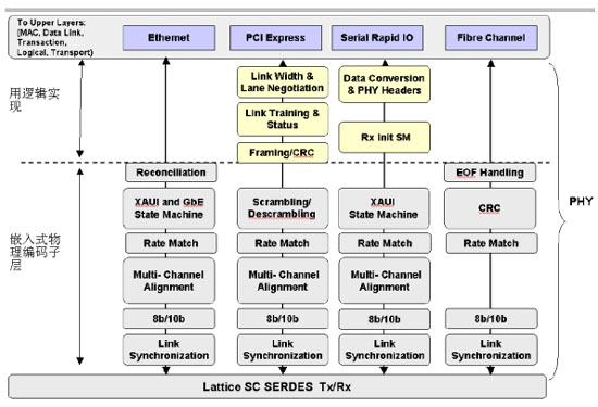
Figure 3: Ethernet, Fibre Channel, PCI Express, and RapidIO Supported by the Physical Coding Sublayer
Memory
In order to support speeds of up to 10 Gbps or higher, the LatticeSC has a large memory block and special circuitry to support standard off-chip memory. The device has 3 levels of memory available for use:
1. On-chip memory: All programmable function units can be configured as RAM or ROM. Users can use basic function blocks to form a small FIFO for local clock domain transfer.
2. Embedded RAM Block: There is a dedicated RAM block array in the device. Used to support packet buffering, large and flexible buffers, and related look-up table memory before and after construction. The total capacity of the embedded RAM block is 7.8Mb.
3. External Memory Interfaces: Some applications require larger memory, such as support for a large number of packet transfers, buffers for traffic management, and long-distance transmission. The sysIO block prefabricates existing and emerging memories with specialized interfaces. Users can choose from a variety of standard interfaces such as DDR1/2, RLDRAM1/2, or QDR1/2. There are DDR circuits in the I/O logic block, along with input delay and dedicated DQS detection circuitry to support the memory interface. The bandwidth per pin can exceed 800 Mbps.
Applications
Figure 4 shows the connectivity role that FPGAs play in today's diverse service environments.
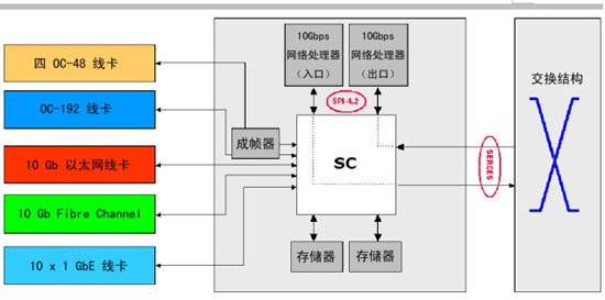
Figure 4: LatticeSC applied to multiple service environments
It can be seen from the figure that a single-chip LatticeSC device can support multiple data streams. LatticeSC devices utilize multiple SPI4.2 cores embedded in a structured ASIC module to seamlessly interface with a 10Gbps network processor. To buffer these faster line speeds, a high-speed memory interface is required. LatticeSC supports all the latest memory standards. Devices with 32 SERDES channels support many serial backplane standards such as SRIO, PCI Express, Ethernet, Fibre Channel, and SONET/SDH.
From above, we can see how LatticeSC meets the challenge of connectivity. On the electrical side, the device has a wide range of interface standards that support the latest memory, network processors, DSPs, and switch fabrics. In order to meet the high-speed serial design, the device has preemphasis at the transmitter and equalization at the receiver to improve signal integrity. High-performance dedicated PLLs can quickly extract clocks from serial streams. The device's physical coding sublayer supports many major protocols.
Product Features
Automatic switch from Boost charge to Floating charge
Constant voltage with current limited
Colorful LCD touch screen - real-time display the working state and running data.
Low output ripple – Makes the charger ideal for all battery types
Full Protection - OVP, OCP, SCP, UTP, reverse connection and other error alarming.
Switching Mode Power Supply,Switching Power Supply,Switching Mode Power Supply 12V,Portable Switch Mode Power Supply
Xinxiang Taihang Jiaxin Electric Tech Co., Ltd , https://www.agvchargers.com