Abstract: MSM6882 is a data modem produced by Japan's OKI company that uses the minimum frequency shift keying method. The device contains receiving, sending and clock generating circuits, and the data transmission baud rate can be selected from 1200bps and 2400bps. The article introduces the main performance and working principle of MSM6882, and gives the application circuit design of MSM6882 in wireless communication.
1 Introduction
The popularity of computers and data terminals has made wireless data communication technology widely used in many fields. In wireless data transmission equipment, the modem is an indispensable part. Modem modulation methods mainly include frequency shift keying (FSK), relative phase shift keying (DPSK), etc. Among them, the minimum frequency shift keying (MSK) modulation method is a better one among the FSK methods. The MSK modulation method is a special case of continuous phase frequency keying (CP-FSK) mode, and its modulation coefficient is 0.5. The MSK signal has no phase mutation at the moment of symbol conversion, so the roll-off of the signal spectrum outside the frequency band will be accelerated, and the occupied frequency band is narrower than that of the PSK signal, but it has the same performance as the PSK signal and is very suitable for use in wireless communication.
MSM 6882 is a modulation and demodulation chip produced by Japanese company OKI that uses MSK modulation. Its working temperature is -25 ℃ ~ 70 ℃, it adopts DIP22 or SOC24 package, its main features are as follows:
â— On-chip filter adopts switched capacitor structure; 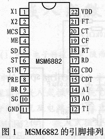
â— Data transmission baud rate 1200 / 4000bps is optional;
â— On-chip transmission filter can be used as an audio signal filter alone;
â— There are two synchronization methods for the receiving timing regeneration circuit for users to choose;
â— The oscillation circuit is integrated in the chip;
â— Modulation can use sine or cosine mode;
â— Adopt single 5V power supply (MSM6882-5).
2 MSM 6882 pin function
The pin arrangement of MSM 6882 is shown in Figure 1, and its pin functions are described as follows:
X1, X2: crystal input pin. When an external clock is connected, X1 is left floating.
MCS: Clock frequency selection terminal. When this pin is "0", the external crystal or clock selects 3.864MHz, and when it is "1", the external crystal or clock selects 7.378MHz.
ME: Modulator enable terminal. When this end is "0", the TI pin is connected to the transmit low-pass filter, and when it is "1", the modulator is connected to the transmit low-pass filter.
SD: Send data input pin.
ST: Send clock output pin. When in use, the rising edge of the ST signal can be used to synchronize the signal of the SD pin.
SIN: Sine modulation method selection.
PRE: Send data preset selection. When it is "0", the SD pin signal is output to the AO pin.
BR: Baud rate selection bit. The selection method is listed in Table 1.
Table 1 Baud rate selection table
| Clock frequency (MHz) | MCS | BR | Baud rate (bps) |
| 7.3728 | 1 | 1 | 2400 |
| 1 | 0 | 1200 | |
| 3.6864 | 0 | 0 | 1200 |
SG: On-chip analog signal ground.
GND: chip power ground.
TI: Audio signal input.
AO: Modulation signal output.
AI: demodulated signal input.
CDT, CDO: chip test pin. In normal use, the CDT pin should be grounded and the CDO pin left floating. 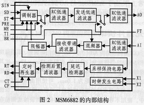
RD: Receive data. The demodulated signal is serially output from this pin.
RT: Receive data clock. When in use, the falling edge of the RT signal can be used to synchronize the RD pin data.
CF: Fast phase lock control. When this end is "1", the phase difference between the output signal of the RD pin and the RT pin is greater than 22.5 °, the phase correction will be completed quickly; if the phase difference is less than 22.5 °, the phase correction will be performed at a low speed. When the pin is "0", regardless of the phase difference between the output signal of the RD pin and the RT pin, the phase correction is performed at a low speed. Under normal circumstances, this pin is connected to high level, that is, select the fast phase lock mode.
CT: Synchronization mode selection. When it is "0", the phase-locked loop completes phase synchronization within 50 bits. When it is "1", the phase-locked loop completes the phase synchronization within 18 bits.
FT: Self-loop test control. Usually connected to high level.
VDD: chip power port.
3 The internal structure principle of MSM 6882
The internal structure of MSM 6882 is shown in Figure 2. The circuit is mainly composed of three parts: sending circuit, receiving circuit and clock generating circuit. The transmission circuit includes a modulator, a transmission low-pass filter, and two RC low-pass filters. It can complete the modulation of the input binary data or the filtering of the input audio signal under the control of PRE and SIN input signals. When completing the modulation function, the modulator first modulates the input data into an MSK signal, and then the high-frequency components are filtered and smoothed by the transmission filter and two RC low-pass filters, and then output to the line. When the audio filtering function is completed, the transmit filter will be disconnected from the modulator and connected to the TI end, thereby directly filtering the input audio signal and sending it to the line.
The receiving circuit is composed of a RC low-pass filter, a mixer, a receiving band-pass filter, a limiter, a sample-and-hold circuit, a delay detector, a detection post filter, and a timing regenerator. After the received signal is filtered by the receiving filter to remove clutter, it can be converted into a square wave signal by the limiter and sample-and-hold circuit and input into the delay detector. The demodulated data is then recovered by the delay detector, sent to the timing regeneration circuit through the detection filter to extract the received clock, and finally the received clock and demodulated data are output.
image 3
The clock generation circuit can provide timing signals for the entire circuit.
4 Application circuit
Figure 3 shows the actual application circuit of MSM 6882. The communication baud rate of this circuit is 1,200 bps. Because both the sending data and receiving data of MSM 6882 need to have a synchronous clock to synchronize, the 82C51 asynchronous serial communication interface chip should be selected to connect the MSM 6882 to the AT89S52 microprocessor. The ATTS of AT82C51 can be used to control the PTT of the radio station, and the RTTS controls the transmission enable of the MSM 6882 through the inverted signal. The SPK pin and MIC pin of the radio station are connected to the AI ​​pin and the AO pin of MSM 6882 through their respective coupling loops. At design time, the input clock cycle of the CLK pin of the 82C51 microcontroller should be in the range of 0.42μs to 1.35μs, otherwise the chip may not work properly. Because the output level of the AOM pin of MSM 6882 is relatively high, the amplitude of the modulation signal input to the radio station can be adjusted through the adjustable resistor W1. The SPK signal coming out of the radio interface is sent to the AI ​​pin of MSM 6882 after signal limiting, and the other is sent to the DSR pin of 82C51 after amplification, detection, and amplitude comparison, as a carrier detection signal. At the same time, the sensitivity of the carrier detection signal is adjusted through W2. When the system detects the signal, it can use delayed transmission to avoid co-channel interference and channel blocking. For the operation method of 82C51, please refer to the related books, which will not be repeated here. For occasions with high requirements for anti-interference, the transmission line transformer can be used to isolate the electrical signals at both ends between the radio station and the modem. Due to space limitations, it will not be repeated here.
Acid Chiller,Sulfuric Acid Chiller,Sulfuric Acid Water Chiller,Acid Copper Plating Screw Chiller
Zhijiang BSL battery technology service company , https://www.bslbatteryservice.com