fsk modulation circuit
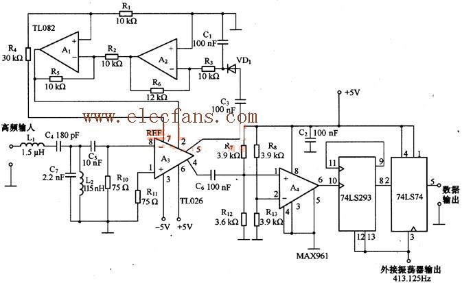
This figure is a FSK modulation circuit composed of 74LS74 and so on. This frequency shift keying (FSK) modulation circuit uses neither a phase-locked loop (PLL) nor a high-Q band-pass filter, so tuning and calibration are not required in this high-frequency modulation circuit. Two tuning circuits can be formed as input filters by L1, L2, C4 and C7, and only the frequency band of the center frequency of lOMHZ is allowed to pass. High-frequency differential amplifier A3, can amplify the signal of lOMHZ. A1 and A2 can form an automatic gain control (AGC) circuit. With the broadband comparator A4, the high frequency signal amplified by A3 can be converted into a digital signal. This digital signal can be used as the clock signal of (74LS293) 4-bit counter. The output of the external oscillator clears the counter. 74LS74 is a D flip-flop, the most significant bit of the counter can be locked on the rising edge of the oscillator output signal. Since the oscillation circuit generates a waveform with a duty cycle of 50%, the two FSK frequencies are 1 = 9.83x10⁶HZ (bit "0") and 2 = 10x106HZ (bit "1"), thereby calculating the oscillation frequency of the external oscillator for 
74LS293 only counts when the oscillator cycle is low. In order to clear the counter, the external oscillator can use crystal oscillator, NE555, etc. The resistance of R10 and R11 should be equal to the impedance of the high-frequency input source. If this FSK receiver is connected to a 50OΩ cable, the resistance of R10 and R11 should be 5OΩ. In this way, the maximum transmission power can be obtained by selecting the resistance value. VD1 can rectify the output voltage of A3 to DC voltage. This DC voltage is amplified and inverted by A2. A1 can invert the output of A2 to provide a positive AGC sink voltage signal. A1 also adds the reference UREF voltage on the A37 pin. The UREF voltage is added to the non-inverting input terminal of A1 through the voltage division of R1 and R4. A4 receives the output signal of the AGC recording system and converts it to a TTL level signal as the clock signal of 74LS293. In order to get the -5V power supply voltage required by the AGC system, the MAX660 can be used to convert the + 5V single power supply to -5V.
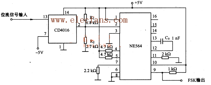
This figure is a FSK circuit composed of NE564 and so on. In the circuit, NE564 is an analog phase-locked loop PLL integrated circuit, which uses a two-state signal to control the CD4016 analog switch for FSK modulation. CD4016 makes the voltage of 2 feet of NE564 switch between 5V and 1.42V, that is 5Vx [R2 / (R1 ten R2)] = 1.42V. The voltage on pin 2 controls the bias current of the phase detector current source. Therefore, in the case of continuous phase, the output of the voltage controlled oscillator (VCO) can be changed. The capacitor C0 that determines the center frequency of the VCO is fixed, and the offset between the FSK frequencies can be adjusted by R1 and R2.
Ip65 Interactive Advertising Player with IP65 front water proof,
with personality, fashion appearance, definitely display
Effect, operating easily.flexible place way, comparison with 10 points Touchwo exclusive touchTechnology, breakthrough the traditional advertising`s space limit of display & play only, challenge the
Simple single touch application. Meet all of your requirements for indoor & outdoor information.
IP65 Interactive Advertising Player
Touch Screen Display,Digital Advertising Player,Indoor Digital Advertising Display,Ip65 Interactive Advertising Player
Guangzhou TouchWo Electronics Co.,Ltd. , https://www.touchaio.com