1 Design of GPS receiver low noise amplifier The main indicators of the designed LNA are: operating frequency is 1 520 ~ 1 600 MHz; noise factor NF
1.1 Device selection Select the appropriate device, considering the low noise figure and high gain, so select PHEMT GaAsFET low noise transistor. Before designing a low-noise amplifier, we must first establish a small-signal model of the transistor. Generally, companies will provide amplifier devices with ready-made models. Here we choose ATF-54143 produced by Agilent. In the 1.52 to 1.60 GHz frequency band, an inverse Ï„ matching network is designed. The matching network consists of lumped element inductance and capacitance. When choosing an inductor, choose a high-Q inductor. In order to be consistent with the actual situation in the simulation, Murata's inductance and capacitance models are used. The chip inductor model selected here is LQWl8, the chip capacitor model is GRMl8, and the inductor LQWl8 at 1.6 GHz has a typical Q value of 80.
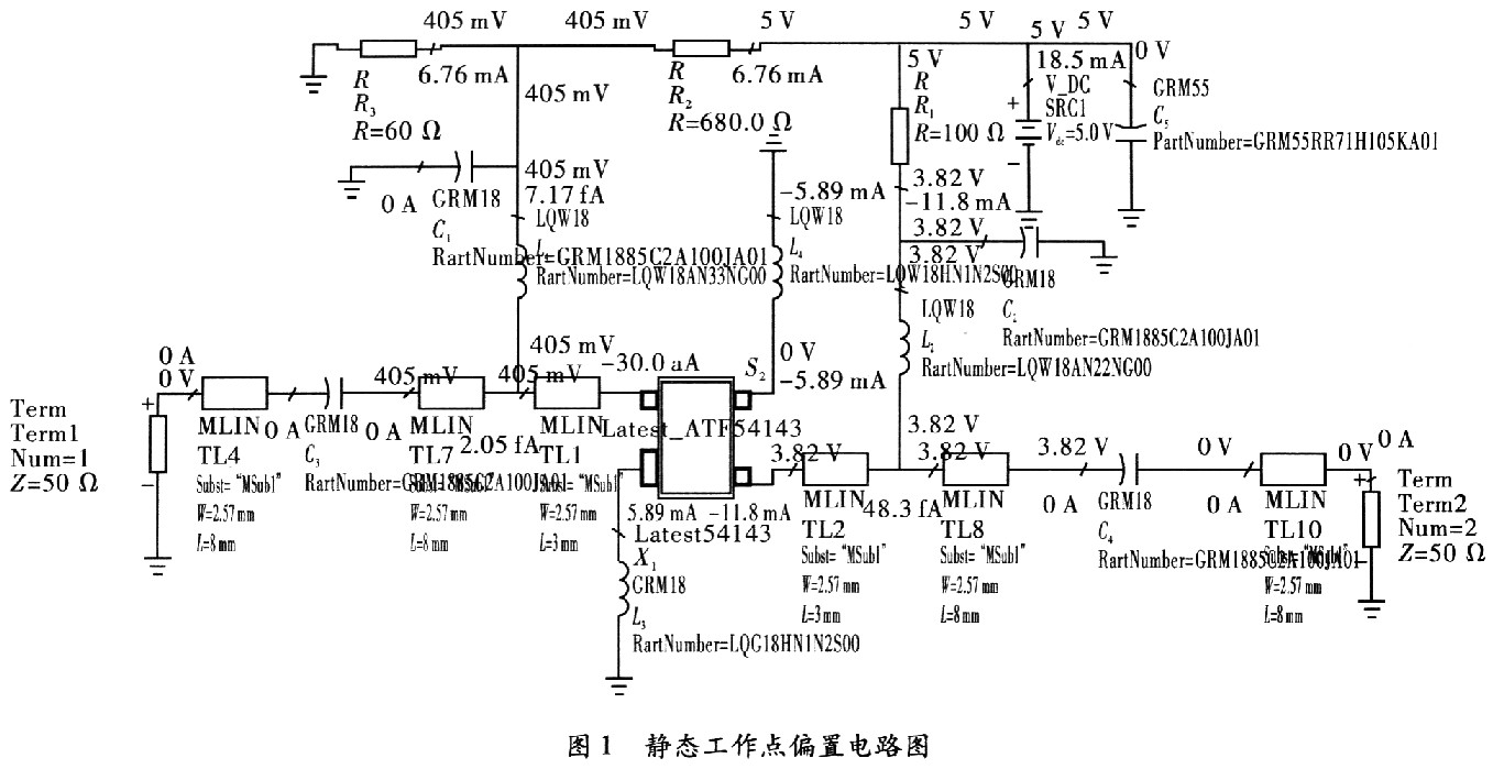
1.2 DC bias In the design of low-noise amplifiers, the goal of designing DC bias is to select a suitable static operating point. The quality of the static point directly affects the noise, gain and linearity of the circuit. A simple bias network composed of resistors can provide a suitable static operating point for ATF-54143, but the temperature is poor. An active bias network can be used to make up for the shortcomings of poor temperature, but the active bias network will increase the circuit size, increase the difficulty of circuit board layout and increase power consumption. In designing the actual circuit, the active bias network or the resistor bias network should be selected according to the specific situation. As for the LNA in the article, considering the structure and cost, the resistor passive bias network is selected here. Using Agilent's ATF54143, the Vds = 3.8 V and Ids = ll mA bias operating points are designed according to the datasheet specifications given by the company. Because ATF-54143 performs better when the current is llmA. The resistance R3 is 100 Ω; R2 is 680 Ω; R1 is 60 Ω, as shown in Figure 1.
1.3 Stability design The stability of the amplifier is an important factor to be considered in the amplifier. It needs to be absolutely stable at the operating frequency. There are two ways to judge that the device is unconditionally stable. the first method 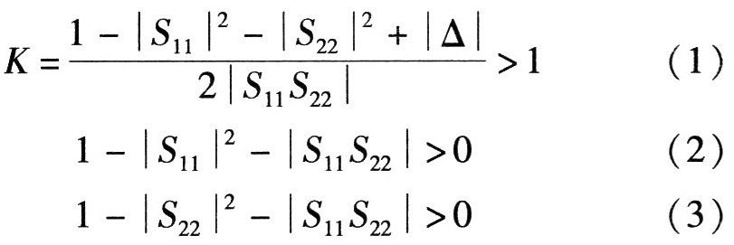
The second method: the detection standard combined with the s parameter has only a single parameter μ, which is defined as 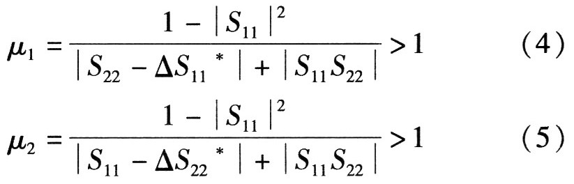
There are usually two methods to stabilize the circuit: the first one is to add a resistive load to the drain end of the field effect tube, which can cause the device to produce equal impedance in a wide frequency band, thereby obtaining broadband stability. The disadvantage is that the resistive terminal consumes some energy and reduces the output power; the second kind, adding an inductance between the source and ground can cause negative feedback in series, which reduces the gain of the device, but the stability is improved. In microwave circuits, the source negative feedback can be an inductive lumped element or a short transmission line. This design uses the former.
The simulation results are shown in Figure 2 and Figure 3. It can be seen that the input and output and the overall stability are> 1 in the range of l 520 ~ l 600 MHz, so the circuit is stable in the band.

1.4 Input and output impedance matching circuit design When designing LNA, input matching can not use conjugate matching method, but the best source reflection coefficient noise matching. The input impedance matching network circuit is composed of C4 and L5. As shown in Figure 3, the network can effectively reduce the return loss and improve the gain and stability in the frequency band. L1 plays the role of passing DC and choke AC, and C1 plays the role of RF bypass. The Q values ​​of the inductors L1 and L5 play an important role in reducing the circuit losses at the input and reducing NF (2). The low inductance Q value will increase the input noise, thereby affecting the total noise of the entire circuit.
The output matching uses a conjugate matching design. The output impedance matching network consists of C6 and L7, as shown in Figure 4, to reduce return loss and increase gain. C2 plays the role of RF bypass, and C5 plays the role of power decoupling.
After using Smith software to obtain the value of the matching network lumped element, optimize it with ADS software. When optimizing, pay attention to several points: First, manually adjust each device parameter through the tuning function to know which device parameters have a greater influence on the circuit index, and handle sensitive device parameters carefully; secondly, set optimization goals; Avoid self-oscillation.
1.5 The overall optimization of the LNA circuit After the DC bias design, stability design and matching network design, the LNA structure is basically fixed, but in order to meet the requirements of various indicators, the value of each device needs to be optimized, and the actual circuit must be considered. With the influence of wire, short circuit grounding, and vias, the overall simulation of the circuit needs to be optimized.
Usually in the radio frequency circuit, the microstrip line is used to transmit signals. It is necessary to pay attention to the width of the microstrip line. The width determines the characteristic impedance. For input and output ports, 50 Ω characteristic impedance is usually used. In this design, the plate chosen is PTFE with a relative constant of 2.65 and a thickness of 1 mm. Using the Appcad software from Agilent, the width of the microstrip line can be calculated to be 2.57 mm.
When optimizing the LNA circuit, the setting of the optimization index should be reasonable. In the process of optimizing the index, we must make full use of the tuning function, first know the approximate value of the parameter, and then optimize each parameter on this basis until the desired effect is achieved. The final simulation result is shown in Figure 5.
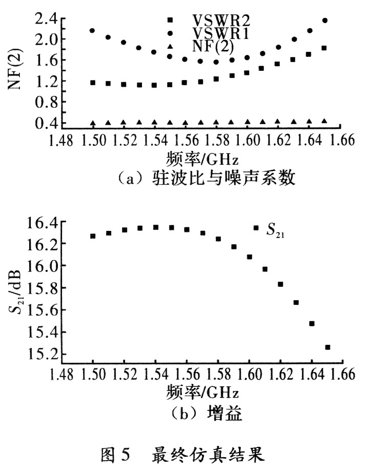
1.6 Test results Figure 6 is the actual low-noise amplifier experiment board, and tested with a vector network analyzer and a noise meter. The test results show that: Gain> 16.0 dB; NF (2) <0.5 dB; input standing wave Ratio <2; output standing wave ratio <1.5. The experimental results are basically consistent with the simulation results.

2 Concluding remarks ATF-54143 with low E-PHEMT noise coefficient from Agilent was selected in this paper to design a low noise amplifier. The design methods of bias circuit, stability design and input-output network matching circuit are introduced. The measured results show that the low-noise amplifier designed in this paper meets the requirements of the index and is suitable for communication in the GPS frequency band.
RCCB named Residual Current Circuit Breaker. When there is human electricity shock or if the leakage current of the line exceeds the prescribed value, Residual current Circuit Breaker/RCCB(without over-current protection) will cut off the power rapidly to protect human safety and prevent the accident due to the current leakage. The rccb switch which made from Korlen electric can be used as infrequent changeover of the line in normal situation.
Korlen electric ---- the rccb switch manufacturer,produces types of Residual Current Circuit Breaker. It is applicable to industrial site, commercial site, tall building and civil house.
Residual Current Circuit Breaker
Residual Current Circuit Breaker,Ac Residual Current Circuit Breaker,Miniature Residual Current Circuit Breaker,Residual Current Electrical Circuit Breaker
Wenzhou Korlen Electric Appliances Co., Ltd. , https://www.korlenelectric.com