Development of the times, technological progress. Various new technologies of digital cameras are emerging one after another, which leads consumers to face the propaganda of the manufacturers or some professional vocabulary in the camera parameter list. Generally, they will feel very difficult to understand, which will affect the judgment before the purchase. Therefore, our digital camera channel has written a series of articles on “Rejecting Professional Terminologyâ€, and strives to explain the common and not easy-to-understand digital camera technology terminology in plain language, so that everyone can clearly understand the relevant technology before purchasing. . In this issue, we will explain the "back-illuminated CMOS sensor" which has a high rate of occurrence, and analyze whether the technology is good or bad.
This article refers to the address: http://
How did the photo come?
The essential value of the camera is to transform the scene that we can see into a flat image that can be preserved, and to turn the fleeting moment into eternity. From another perspective, this is a way of energy flow. The job of the camera is to convert the light energy into a medium and convert it into information storage.
Among them, film camera imaging relies on the chemical characteristics of silver halide crystals, that is, chemical changes occur when light is encountered, and images are obtained through a series of processes such as rinsing. The specific details are not developed.
Technology has developed into the era of digitalization. The storage of photos is ultimately in the form of numbers, which is a series of numerical values. What kind of process does it take from the light of nature to the digital picture file?

Digital photos are the result of some circuits and software calculations
Photographs need to be represented in a digital way. A very important step is quantification, which means that we need to transform the natural scene into a way that can be accurately measured in terms of numerical values. In fact, the core component of the quantization process is the image sensor, which can convert the light of different strengths and different colors transmitted to it into a photoelectric diode (photodiode) for photoelectric conversion into electric charge or voltage information. The entire image sensor All the information on the dot matrix comes out to the processing chip to generate a picture in digital format.
CCD sensor and CMOS sensor
The two kinds of image sensors that are commonly used nowadays are the CMOS and CCD sensors that we have often heard. In order to let everyone finally understand the back-illuminated CMOS sensor, Xiaobian here also briefly talks about the similarities and differences between the two sensors. Advantages and disadvantages. As shown in the figure below, the left side is the structure of the CCD sensor, the right side is the mechanism of the CMOS sensor, and the small yellow square is the pixel point.
As can be seen from the figure, the charge data of each pixel in each row of the CCD sensor is sequentially transferred to the next pixel, outputted by the bottommost portion, and amplified by the amplifier at the edge of the sensor; In the sensor, each pixel is adjacent to an amplifier and A/D conversion circuit, and the data is output in a manner similar to a memory circuit. To put it simply, there are different ways to treat the charge data obtained at a single pixel. The CCD is all transmitted and then processed uniformly. The CMOS is processed separately. These two methods are not imagined by people, but by the manufacturing process of CCD and CMOS. Because the data transmitted in CMOS devices will have high distortion, it needs to be processed first.
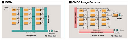
Difference between CCD sensor and CMOS sensor
Because of the difference in processing between the two sensors, in the early days, CMOS image sensors were worse than CCD in terms of sensitivity, resolution, and noise control, but the advantages were low cost, low power consumption, and high integration. Features, especially suitable for more articles on the number of pixels can be improved. Therefore, in recent years, chip-level manufacturers have put a lot of energy on CMOS sensors, so that CMOS sensors now occupy a very high share of market end products, especially digital cameras.
Basic principle of back-illuminated CMOS sensor
Time advances to June 2008, Sony released a back-illuminated CMOS, and the Exmor R name, and first used in several DV products. Back-illuminated CMOS images have been rapidly developed since then. Many chip manufacturers have released this type of products, and more and more digital imaging devices have adopted this technology. Next, Xiaobian will elaborate on the characteristics of this technology.
The biggest optimization of the back-illuminated CMOS sensor is to change the internal structure of the component, that is, to adjust the direction of the component of the photosensitive layer, so that the light can be directly injected from the back, avoiding the traditional CMOS sensor structure, the light will be affected by the microlens and the photoelectric The effects of circuits and transistors between the diodes significantly improve the performance of the light and greatly improve the shooting in low light conditions.
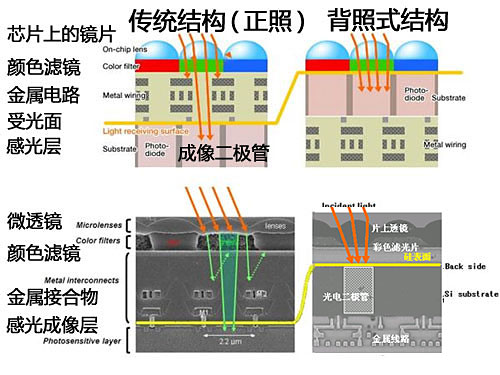
Back-illuminated CMOS sensor physical structure
The specific structure of the back-illuminated CMOS sensor is shown in the above figure (from Sony's data, the products of other chip manufacturers may differ in details, but the general meaning is the same), the orange is the optical line, and the yellow line is the light-receiving surface. The traditional style on the left clearly shows that after the light passes through the microlens, it needs to pass through the circuit layer to reach the light receiving surface, and the light in the middle will inevitably suffer partial loss (including being blocked or weakened). The components of the back-illuminated CMOS sensor are different. After the structure is changed, the light passes through the microlens and can directly reach the back side of the photosensitive layer, completing the photoelectric reaction, and improving the photosensitive process from the amount of light entering.
Then we analyze it more carefully. Since there is no barrier in the middle, the photosensitive surface of the back-illuminated CMOS sensor is closer to the microlens, that is, the incident angle and the covered surface of the light can be optimized, and the photosensitive element may output more. For excellent signal.
Based on the above factors, the back-illuminated CMOS sensor has a qualitative leap in sensitivity compared with the conventional CMOS sensor. As a result, the focusing ability and image quality are greatly improved under low illumination.
Why is it so late to introduce back-illuminated CMOS?
Why do seemingly simple improvements be made in the traditional CMOS sensor for so long? In fact, scientists thought about it 20 years ago, because the structure-adjusted back-illuminated CMOS sensor has very high requirements on the production process and micro-processing technology of electronic devices, because this technology requires the substrate carrying the diode to be very thin. Probably 1/100 of the thickness of a conventional positive-illuminated CMOS sensor substrate. Therefore, when the chip manufacturer does not have enough internal control, it is inevitable that the back-illuminated CMOS sensor will not be worth the loss, which may lead to more noise.
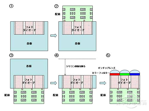
Back-illuminated CMOS sensor production process
What are the advantages of the new back-illuminated CMOS sensor?
The new back-illuminated CMOS sensor has benefited from the upgrade of the manufacturing process of electronic devices, at least in two aspects. The first one is that the performance of the microlens on the sensor is further improved, so that the light passing through the microlens is incident on the photosensitive surface at an angle closer to vertical, and the adverse effects such as dispersion, glare, etc. generated by the microlens are weakened, and finally The light reaching the sensor's photosensitive surface is better than the conventional one. The second is that it still has high-speed processing power under large pixels, which is in the final analysis compared to CCD sensors. The CCD sensor needs to transmit the charge data of each pixel to be processed uniformly, so the speed is hard to increase when the pixel is large, and the noise is increased if the processing bandwidth is forcibly increased. The CMOS sensor has converted the charge into voltage data at every pixel, and there is a relatively large space for increasing the frame rate of large pixels.
However, these two advantages are not unique to the CMOS sensor, which is common in today's new CMOS sensors. This is why more and more digital cameras use CMOS sensors. After all, the performance of large pixels and high speed will directly affect. The choice of the end consumer.
Would it be better to use a back-illuminated CMOS sensor?
Since the back-illuminated CMOS sensor is so powerful, is it true that the digital camera equipped with it is very good? In fact, it is not, in addition to the core component sensor, there are factors such as lens and processing algorithm. The factors of the lens should be easy to understand, because the light is passed through the lens before it reaches the sensor. The lenses used in each model are not the same, and the specific quality will of course vary. The other is the aspect of data processing, because the data from the sensor is still processed by the processor inside the digital camera to get the final photo data (except for the camera that can output RAW format), in other words, the original material. Also need to do the touch to get the finished product. This part depends on the image processing algorithms of various manufacturers. This is like the cooking methods used by different chefs to process ingredients. The final picture will use different qualities and different styles.
Comparing the ISO quality of the cameras equipped with back-illuminated CMOS sensors and other cameras, the general conclusion is that at low ISO, the difference between the two is small, but there is a certain improvement at high ISO. It is also worth mentioning that the camera equipped with a back-illuminated CMOS sensor has a greatly enhanced focusing ability in low-light environments, which is a very important upgrade.
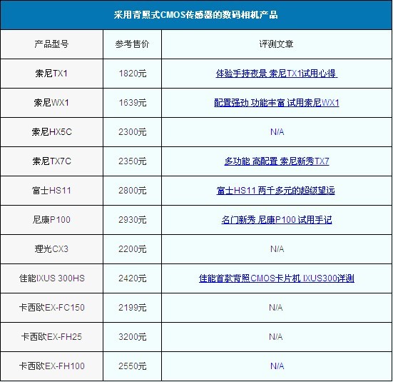
Camera models currently using back-illuminated CMOS sensors on the market
Summary: So far, a number of chip manufacturers have announced their own back-illuminated CMOS sensor products, and then there will be more impact products using back-illuminated CMOS sensors, including Apple's latest release of iphone 4 Generation mobile phone. This article introduces some of the basic principles of back-illuminated CMOS sensors and solves some common problems. I hope to have practical help for netizens who are ready to buy digital cameras.
Outdoor Led Display is a new form of media advertising,is a perfect combination between new media technical and Outdoor Led Display advertising publishing , Outdoor Led Display advertising is use light-emitting diodes spelled to show advertising words or pictures; Mainly used in shopping malls, squares, airports, railway stations, hotels and other places, with bright, waterproof, long life, large perspective, viewing distance and so on, Shenzhen Cxcolor optoelectronics Co.,ltd is professional produce LED display, LED stage rental screen, advertising LED display, small spacing LED display,Outdoor Led Display, led transparent screen, car Led Screen, led ball screen, led energy-saving screen, etc., to supply customers a complete set of LED display solutions

Outdoor Led Display
Outdoor Led Display,Led Display,Outdoor Led Display Board,Led Outdoor Display
Shenzhen Cxcolor Optoelectronics Co., LTD. , http://www.largeledscreen.com