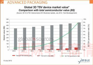
 Market research agency Yole Developpement earlier released a survey report for 3DIC and TSV, pointing out that all 3D or 3D-WLCSP platforms (including CMOS image sensors, ambient light sensors, etc.) in TSV packages have been used in the past year. The output value of products such as power amplifiers, radio frequency and inertial MEMS components is approximately US$2.7 billion. By 2017, this figure is expected to grow to US$40 billion, accounting for 9% of the total semiconductor market.
 Lionel Cadix, market and technology analyst for advanced packaging at Yole Developpement, points out that 3DIC usually uses TSV technology to stack memory and logic ICs. It is expected that such components will grow rapidly; in addition, 3D WLCSP will also have a compound annual growth rate of 18% ( CAGR) grows quickly.
In 2017, 3D TSV chips will account for 9% of the total semiconductor market.
TSV
3D WLCSP: The most mature 3D TSV platform 3D WLCSP is the current preferred solution for integrating small-size optoelectronic components such as CMOS image sensors. It is also the most mature 3D TSV platform. Yole Developpement estimates that the market size will be about 270 million US dollars in 2011, of which more than 90% comes from low- and low-resolution CMOS image sensors (usually CIF, VGA, 1MPx/ 2MPx sensors, etc.) Taiwan's Xintec is the current leader in 3D WLCSP packaging, followed by China WLCSP, Toshiba and JCAP.
Most 3D WLCSP operators are based on 200mm wafer-level packaging services. However, all major players have shifted towards 300mm. In fact, this trend is also a necessary process for the high-order CMOS image sensor market (>8MPx resolution). The current sensor market is also shifting from backside illumination to the real 3DIC package architecture. This latest architecture is called "3D BSI", in which the photodiodes are stacked vertically directly on the DSP/ROIC wafer and connected via TSV.
Future 3DIC will be Driven by Memory and Logic Stack SoCs In the coming decades, 3DICs will become the new model of the future semiconductor industry by virtue of their lower cost, smaller size, and advancement of chip functionality. Jerome Baron of Yole Developpement's Advanced Packaging Business Group points out that in the next five years, 3D stacked DRAM and 3D logic SoC applications will become the most important driving force for the adoption of 3DIC technology, followed by CMOS image sensors and power components. And MEMS and so on. He said that today's high-end applications are still 2.5D silicon interposer technology. Thanks to the advanced chip design and packaging technology, more large-scale FPGAs and ASICs have already begun to be used in the industrial field, and will also be used in markets such as games and smart TVs in the future.
In 2013, 3DIC technology is expected to grow significantly under the drive of memory companies such as Micron, Samsung, SK-Hynix, and IBM and other high-performance computing equipment suppliers.
However, it may not happen until 2014 or 2015 when the so-called wide I/O interface and TSV technology at 28nm are used to mass-produce a dedicated application processor chip for mobile/tablet products. In fact, to successfully promote 3DIC, apart from technical issues, it also involves a complex supply chain, and it has a lot of layers to change. As a result, foundry giants including Samsung and Taiwan Semiconductor Manufacturing Co., Ltd. (TSMC) have continued to implement vertical integration for 3DIC, hoping to meet leading fabless semiconductor companies such as Qualcomm and Broadcom. , Marvell, NVIDIA, and Apple's needs, as well as other companies that have adopted fab-fabrication strategies such as Texas Instruments, STMicroelectronics, and NEC/Renesas.
Jean-Marc Yannou, senior analyst of advanced packaging department of Yole Developpement pointed out that the semiconductor packaging, assembly and testing market of 3D TSV will reach 8 billion US dollars in 2017. "In the future, when expanding 3DIC business, the industry must seek the so-called "virtual IDM" model," he pointed out, including the TSV etching filling, wiring, bumps, wafer testing and wafer level assembly including the intermediate wafer processing department The market size is expected to reach 3.8 billion U.S. dollars. In addition, the assembly and testing parts of the latter stage, such as the 3DIC module, are estimated to reach US$4.6 billion, and these represent business opportunities for the sustainable growth of the advanced packaging industry in the future.
Sensor Dustbin Automatic Dustbin
Sensor Dustbin Automatic Dustbin,Automatic Sensor Recycling Dustbin,Stainless Steel Sensor Automatic Dustbin,Automatic Sensor Dustbin
NINGBO ZIXING ELECTRONIC CO.,LTD. , https://www.zixingautobin.com