Cheap "watchdog" design (Schmidt trigger)

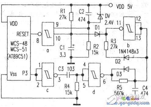
This circuit is designed for use in single-chip systems such as the MCS-51 series. The electrical schematic is illustrated in the diagram below. In the figure, a four-input "2-NAND" Schmitt trigger 74HC132 is used. Gates C, D, B, along with components like C3, C4, R4, R5, D3, and D2, form the core of the circuit.
Cheap "watchdog" design (Schmidt trigger)
Unlike traditional "watchdog" circuits that rely on oscillators, this design uses a different approach. Gates C and C3 are isolated, allowing the input of gate C to be connected to an I/O pin that frequently toggles during the main loop of the system's program. Because it’s a CMOS high-impedance input, it doesn’t interfere with the I/O pin’s normal function. For example, you could use P3.7 and include an instruction like CPL P3.7 in the main loop to toggle the pin—outputting a high level, then a low level, and repeating. This causes the output of gate C to constantly change, which in turn affects the output of gate D. When the output of gate D (pin 6) is high, C4 charges through R5. When it goes low, C4 quickly discharges through D3. As long as the main loop runs normally, the I/O pin keeps toggling, keeping the output of gate D changing continuously. This means C4 remains at a low level, which is applied to gate B, causing its output (pin 10) to stay high. This prevents D1 and D2 from activating, so the rest of the circuit remains unaffected, and the system continues operating normally. However, if the system crashes or the program gets stuck, the I/O pin stops toggling. Gate C’s input remains at a constant high or low level. Due to the isolation provided by C3, the inputs of gate D (pins 4 and 5) are pulled down by R4, causing the output of gate D (pin 6) to stay high. C4 then charges through R5. After approximately 500 milliseconds, the output of gate B (pin 11) drops low. This triggers C1 to discharge quickly through D1, bringing the output of gate A (pin 8) high, which resets the CPU. At the same time, C4 discharges through D2 and R3. Once C4 reaches the VL threshold, gate B flips, causing its output (pin 11) to go high again. This blocks D1 and D2, allowing C1 and C4 to start charging through R1 and R5 respectively. Since the time constants of R1 and C1 are much shorter than those of R5 and C4, gate A flips first, sending a low signal to its output (pin 8), which resets the CPU. Once the main loop resumes normal operation, the input of gate C starts toggling again, and the circuit returns to a stable state. Additionally, gate A, along with resistors R1 and R2, capacitors C1 and C2, and Zener diode DW, forms a voltage monitoring circuit. R1 and C1 are primarily used for power-on automatic reset. During system startup, gate A’s output (pin 10) is low, generating a reset pulse to initialize the CPU. C2, R2, and DW on gate A’s pin 9 provide power-failure protection. At power-up, C2 holds pin 9 high. Once the power stabilizes, the Zener diode clamps the voltage at 2.6V (5V - 2.4V). The Schmitt trigger ensures that pin 9 remains high, preserving the original state of gate A. If the power supply drops below 4V, the voltage at pin 9 falls to 1.6V, triggering gate A to flip and send a high signal to pin 8, resetting the CPU. This prevents any unintended behavior during power-down or under-voltage conditions, ensuring safe operation once power is restored.

Inductors

I-Beam Inductors,Chip Inductors,Color Ring Inductor,R-Bar Inductors

Shenzhen Sichuangge Magneto-electric Co. , Ltd , https://www.scginductor.com

This entry was posted in on