Modern radar signal processing has become a critical component in achieving the full functionality of radar systems. This paper presents a systematic optimization of both the hardware architecture and software design of a radar signal processor, tailored to meet specific system requirements. A core signal processing board is designed using four TS201 chips and one FPGA, enabling two-dimensional space-time signal processing with just a single sub-board. The system supports key algorithms such as adaptive sidelobe cancellation, four-way pulse compression, MTI/MTD, sidelobe shadowing, and differential beam angle measurement, allowing accurate calculation of target distance and azimuth deviation to fulfill the system’s operational needs.
**1. System Composition Analysis**
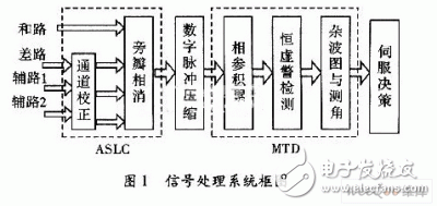
The echo signal is partially combined with microwave signals from the antenna to form sum and difference channel signals, along with two auxiliary antenna signals for IQ orthogonal interpolation. After 1/8 decimation, four test data channels are generated at a data rate of 128 MB/s. The system algorithm structure, as shown in Figure 1, consists of three main modules: a sidelobe cancellation module, a digital pulse compression module, and an MTD processing module. Once the sum signal undergoes MTD (FFT-CFAR), the azimuth deviation is calculated based on the sum and difference data when a target is detected.
Taking the low-frequency operation mode of the radar as an example, the IQ data contains 5,388 points with a repetition frequency of 140 Hz. Considering a certain time margin, the transmission and processing of four signals must be completed within 6.7 ms. Therefore, the system's data rate, data volume, and computational scale necessitate the following characteristics:
(1) High-performance floating-point processing chips capable of handling sidelobe cancellation, pulse compression, coherent accumulation, clutter map generation, and constant false alarm rate processing.
(2) High-speed internal data transfer between chips and external memory expansion to manage large amounts of data efficiently.
(3) External data and control interfaces, with the ability to output fault detection signals.
(4) Extensive software optimizations to ensure all processing modules complete within a single pulse period.
**2. Radar Processor Implementation**
**2.1 Hardware Platform Design**
Given the high computational load and strict timing requirements, the signal processing board employs a multi-DSP parallel processing architecture. To achieve high-speed floating-point processing, high data throughput, and sufficient memory capacity, the ADSP-TS201 chip from Analog Devices is selected. It features a 600 MHz operating clock, executing up to four instructions per cycle, with dual independent arithmetic blocks and dual integer ALUs for address calculations. The chip also includes 24 MB/s of on-chip memory, 14 DMA controllers, and four link ports for high-speed data transfer.
Multi-DSP designs typically use either shared bus or link port coupling. While shared bus structures offer a global address space, they suffer from bus contention during frequent data exchanges. In contrast, link port coupling provides independent memory spaces for each DSP, simplifying program debugging and reducing PCB complexity. Data transfer via link ports uses DMA, avoiding CPU overhead and improving real-time performance. Four TS201s are interconnected through link ports, forming a loosely coupled multi-DSP system capable of transferring up to 500 MB/s between any two DSPs.
The board primarily uses four TS201s and one FPGA as the core components, along with FLASH, SDRAM, and fiber interface chips to handle data storage and transmission. The FPGA manages timing control, external data transmission, and bus communication with the DSPs. It connects to DSP0 and DSP1 via two independent 32-bit buses, operating at 50 MHz to achieve 400 MB/s data transfer speeds. The system clock runs at 50 MHz, with the TS201 operating at 600 MHz (12x). The peak processing capability of the single board reaches 14.4 Gflops, meeting the system's performance requirements.
**2.2 System Software Design and Optimization**
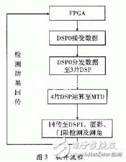
Due to the complexity of the system algorithms and dynamic range requirements, the software is implemented on the DSP for ease of debugging. After microwave synthesis, the sum, difference, and two auxiliary channel signals are formed. After A/D sampling of the orthogonal difference, the four-channel data is transmitted to the FPGA via optical fiber, and then distributed to the other three DSPs via the bus. Each DSP processes one channel independently, as shown in Figure 2. After MTD processing, the data is sent back to DSP1 for sidelobe and threshold detection, estimating the target’s azimuth deviation. The detection result is returned to the FPGA via DMA, completing the module within one pulse period, as illustrated in the software flow diagram of Figure 3.
**(1) Digital Pulse Compression**
Digital pulse compression enhances the radar’s resolution and signal-to-noise ratio by processing the received signal with a matched filter. This technique allows for longer pulses that carry more energy while maintaining high range resolution, making it essential for modern radar systems.
Solar Inverter
A solar inverter converts direct current (DC) electricity from solar panels into alternating current (AC) for use in homes and businesses.
Usage:
Solar inverters are used in both residential and commercial solar power systems to convert the electricity generated by solar panels into a usable form for powering homes, businesses, and other facilities. They are an essential component of grid-tied solar systems, off-grid solar systems, and hybrid solar systems.
Working Principle:
Solar inverters work by using a process called "pulse width modulation" to convert the DC electricity generated by solar panels into AC electricity. This involves rapidly switching the DC input to create a waveform that mimics the characteristics of standard grid electricity. The inverter also synchronizes the output with the grid frequency and voltage to ensure compatibility with the existing electrical infrastructure.
Purpose:
The primary purpose of a solar inverter is to enable the use of solar energy as a practical and reliable source of electricity for residential and commercial applications. By converting the DC electricity generated by solar panels into AC electricity, solar inverters make it possible to power appliances, lighting, and other electrical devices with clean, renewable energy from the sun. Additionally, solar inverters also provide monitoring and control functions to optimize the performance and efficiency of the solar power system.
solar inverter, photovoltaic inverter, grid-tie inverter, off-grid inverter, renewable energy converter
Bosin Power Limited , https://www.bosinsolar.com