Abstract: Based on the NXP Class-D TFA9810T chip, a stereo-functional green energy-efficiency analog Class-D power amplifier design is realized. The audio amplifier is mainly composed of a fully differential input and a full-bridge BTL output structure for dual-channel power amplifiers and second-order Butterworth. Filter construction. The topology structure of analog class D power amplifier system, PWM modulation, input and full bridge output, negative feedback, LPF filter circuit design are introduced in detail, and the elements of dead zone correction, EMI suppression and PCB layout design are mainly discussed. Simulation tests show that the power amplifier can supply 10 W×2 output power to two 8 Ω speakers at a supply voltage of 15 V. The actual conversion efficiency can reach 90%, the total harmonic distortion is less than 7%, and the 1 kHz sine wave audio output is not paid. The more distortion, no obvious EMI interference, the relative temperature rise of the power amplifier housing is 25 °C.
Key words: Class D power amplifier; green energy efficiency; full bridge; electromagnetic interference; printed board
This article refers to the address: http://
0 Introduction In the multimedia era, traditional Class A, Class B, and Class AB linear analog audio amplifiers cannot meet the requirements of electronic audio-visual LCD/PDP/OLED/LCOS/PDA, etc. due to their low efficiency and high energy consumption. New development trends, and non-linear audio amplifier parts Class-D power amplifiers will be included in more and more new product designs due to their advantages of energy saving, high efficiency, high output power, low temperature rise, and small footprint. The class D amplifier architecture is divided into a half-bridge asymmetric type and a full-bridge symmetrical type, while the full-bridge type has a four-fold output power with respect to the half-bridge type, which is more efficient; from the signal adaptation to the analog type and the I2S all-digital type, Because the all-digital type is still in the development stage, the cost is high, and the analog type will be in the mainstream of application in the next few years due to the cost advantage. This paper focuses on the design elements of the full-bridge analog type D power amplifier, and realizes a circuit design based on NXP's new green energy efficiency analog class D power amplifier TFA9810T, focusing on green energy-saving high efficiency, high output power, low temperature rise effect, PCB layout, Several aspects of EMI suppression are summarized and analyzed.
1 Class D power amplifier principle features
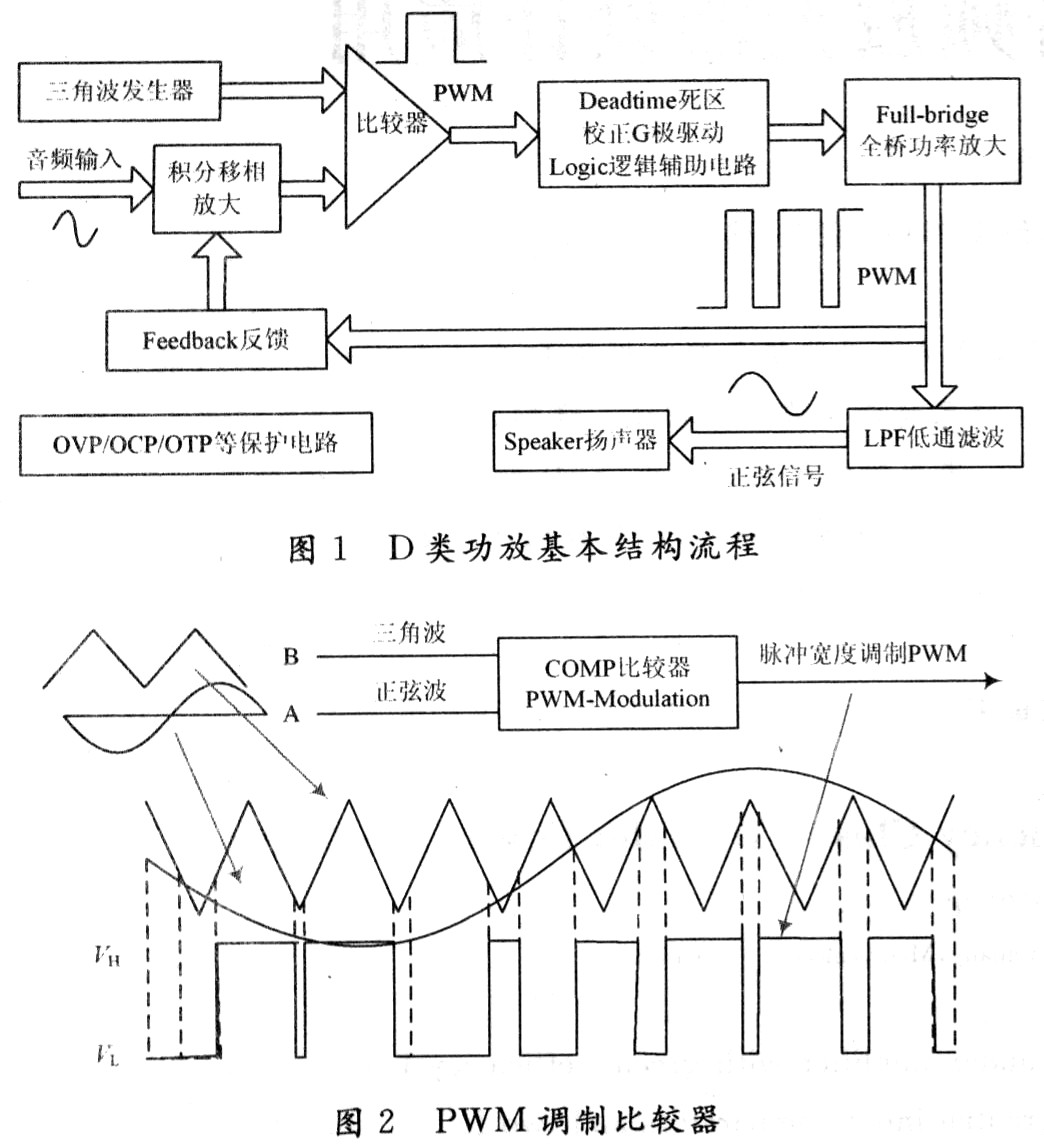
1.1 Class D Amplifier System Structure Class D amplifier consists of integral phase shifting, PWM modulation module, G gate drive, switching MOSFET circuit, Logic auxiliary, output filtering, negative feedback, protection circuit and so on. The process first modulates the analog input signal into a PWM square wave signal, and the modulated PWM signal drives the power output stage through the driving circuit, and then filters the high frequency carrier signal through low-pass filtering, the original signal is recovered, and the speaker is sounded, as shown in the figure. 1 is shown.
1.2 Modulation level (PWM-Modulation)
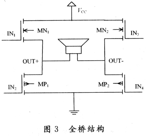
The modulation stage is A/D conversion, which samples the input analog audio signal to form a high-low level digital PWM signal. In Figure 2, the comparator's non-inverting input is connected to the audio signal source, and the opposite end is connected to the triangular wave signal generated by the internal clock of the power amplifier. When the signal level of the audio input is higher than the triangular wave signal, the comparator outputs a high level VH, and vice versa, outputs a low level VL, and converts the input sine wave signal into a PWM wave whose width varies with the amplitude of the sine wave. This is one of the cores of Class D power amplifier. It must require the linearity of the triangular wave to be good, the oscillation frequency is stable, the comparator has high precision and high speed, and the PWM square wave rises and falls sharply. The deep modulation measures are described in the literature [2].
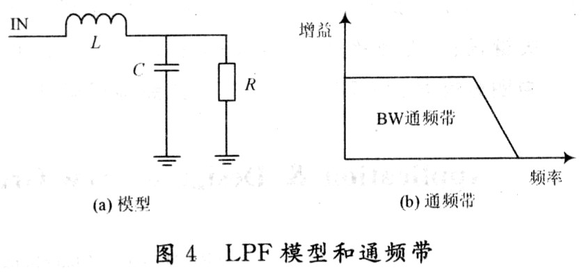
1.3 Full-bridge output stage The output stage is a switching amplifier with an output swing of VCC. The circuit structure is shown in Figure 3. The MOSFET is equivalent to an ideal switch. When turned off, the on-current is zero, no power consumption; when turned on, the voltage at both ends is still close to zero. Although there is current, the power consumption is still close to zero; the whole work Cycle, MOSFET has basically no power consumption, so theoretically the conversion efficiency of Class D power amplifier can be close to 100%, but considering the auxiliary circuit power consumption and MOSFET conduction loss, the overall conversion efficiency is generally about 90%. Because the conversion efficiency is very high, the heat energy consumed by the chip itself is small, and the temperature rise is also very small. It can be completely ignored without considering heat dissipation, so it is called a green energy efficiency class D power amplifier.
For the full bridge, further reduce the conduction loss, so that the on-resistance RON of the MOSFET drain source is as small as possible. The MOSFET with low switching frequency and small gate-source capacitance is selected to enhance the driving capability of the pre-driver.
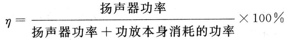
1.4 LPF low-pass filter-level LPF filter can eliminate electromagnetic interference and switching signals in PWM signals, improve efficiency, reduce harmonic distortion, directly affect amplifier bandwidth and THD, must set appropriate cutoff frequency and filter roll-off coefficient, Guarantee audio quality. For audiovisual products, 20 Hz to 20 kHz is audible; below 20 Hz is infrasound; above 20 kHz is ultrasound. In applications, the cutoff frequency is generally set to 30 kHz. The lower the frequency, the narrower the signal bandwidth, but too low will damage the signal quality. If it is too high, there will be noise mixing. Commonly used LPF filters generally include three types: Butterworth filter, Chebyshev filter, and Kaul filter. The Butterworth filter has good maximum flat amplitude characteristics in the passband BW, and is easy to implement. Therefore, the LC second-order Butterworth filter with small equivalent internal resistance and large output power is shown in Fig. 4.
1.5 Negative feedback Negative feedback is an LPF circuit that feeds back the detected audio components of the output stage to the input stage, compares it with the input signal, compensates, corrects, and shapes the output signal to improve the linearity of the amplifier and reduce the power supply. Ripple (power supply rejection ratio, PSRR). Negative feedback can reduce the noise generated in the passband due to pulse width modulation, output stage and power supply voltage variation, so that the low-frequency components in the output PWM can always be consistent with the input signal to obtain a good THD, which makes the sound more abundant and accurate.
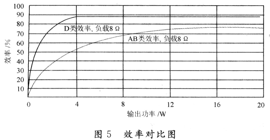
1.6 Power efficiency analysis Class D efficiency can reach more than 85% efficiency under the condition of THD<7%, which is much higher than the linear theoretical power amplifier with the maximum theoretical efficiency of 78.5%. The root cause is that the output stage MOSFET is fully operational in the switching state. In theory, Class D power amplifier efficiency is:
Assuming that the on-resistance of the class D power amplifier is RON, all other passive resistors are RP, the filter resistance is RF, and the load resistance is RL, the efficiency of switching loss is not considered:
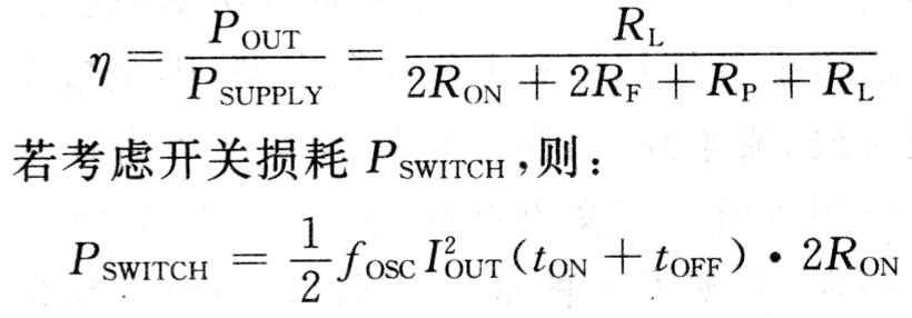
Where: fOSC is the oscillator frequency; tON and tOFF are the MOSFET on and off frequencies, respectively. The efficiency at this time is: 
According to the above formula, the load RL in the class D power amplifier is higher in efficiency than the other resistors. The MOSFET is used as a freewheeling switch, and the power consumed is almost equal to the sum of the I2RON loss and the quiescent current on the MOSFET's on-resistance. The power output to the load is almost negligible. Therefore, its efficiency is much higher than that of a linear power amplifier, as shown in Figure 5. It is very suitable for today's green energy-saving requirements, and is suitable for use by digital audio-visual products such as tablets.
2 Key Points to Pay Attention to Class D Power Amplifiers Note the following points in Class D design applications:
2.1 Deadtime (dead zone correction)
The full-bridge MOSFET is turned on in pairs, ideally, one pair is turned on and the other pair is turned off, but in fact, there is a process in which the power tube is turned on and off. During the transition, there must be a moment. As shown in Figure 3, IN2/IN4 has started to turn on when IN1/IN3 has not been completely turned off. Because the MOSFETs are all connected across the power supply, it may be in extreme time. A large voltage and current are simultaneously applied to the four MOSFETs, resulting in large power consumption, a decrease in overall efficiency, and an increase in temperature rise of the device, which burns out the MOSFET and reduces reliability. In order to avoid the two pairs of MOSFETs in the same state, causing a large potential short-circuit current, it should ensure that a pair of MOSFETs are turned on and another pair of MOSFETs have a short dead time (Dead-time). This time is controlled by the Logic logic controller to effectively ensure that one set of MOSFETs is turned off and the other set of MOSFETs is turned on at the appropriate time to reduce MOSFET losses and improve amplifier efficiency.
However, if the Deadtime is not set properly, the following problems will occur:
(1) A glitch will be generated in the output signal, causing electromagnetic interference, that is, IN1/IN3 is turned off during the dead time. The fully out-of-control output voltage will be affected by the body diode current in Figure 6(a) (body diode current formation, see EMI section below), and glitch interference will appear in the output waveform.
(2) Deadtime is too large, the energy contained in the output glitch will continue to be consumed in the body diode, consuming energy in the form of thermal energy, which seriously affects the chip's working stability and output efficiency.
(3) Deadtime is too long, affecting the linearity of the amplifier, causing the output signal to cross the distortion. The longer the time, the more serious the distortion.
2.2 EMI (Electro-Magnetic Interference)
EMI is mainly formed by the reverse recovery charge of the MOSFET body diode. The specific generation mechanism is shown in Figure 6.
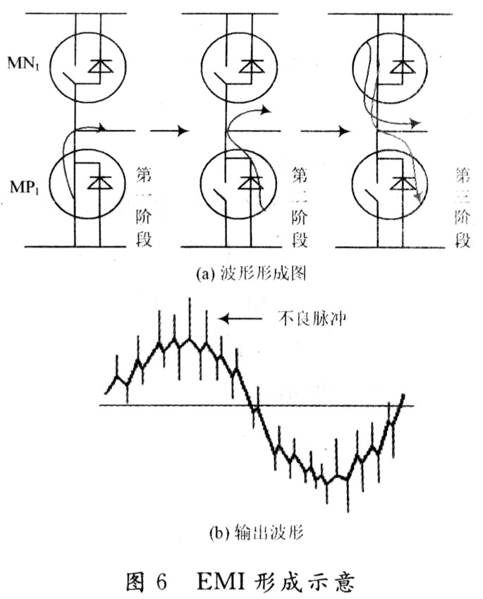
In the first stage, the MP1-MOSFET is turned on, and current flows through the MOSFET and the LPF inductor. In the second stage, during the completion of the full-bridge, the MP1 itself is turned off, but the body diode is still turned on to ensure the in-stage inductance. In the third stage, the Deadtime period ends, and the MN1 turns on. If the remaining charge stored in the MP1 body diode has not been completely released, the stored charge that was not released during the last conduction period is instantaneously released, resulting in a surge in reverse recovery current. This current tends to form a sharp pulse that is ultimately reflected in the output waveform, as shown in Figure 6(b). Therefore, the output spectrum will contain a large amount of spectral energy at the switching frequency and the switching frequency multiplier, forming EMI externally.
In order to suppress EMI, in order to reduce the output square wave frequency and slow down the top wave of the square wave, some new internal EMI elimination circuit technologies are applied to new products:
(1) Dither. Spread spectrum technology, that is, periodically adjust the frequency of the triangular wave sampling clock within the specified range, and the fundamental wave and the higher harmonics avoid the sensitive frequency band, so that the output spectrum energy is flat and dispersed;
(2) Increasing the active radiation limiting circuit, actively controlling the output MOSFET gate when outputting transients, to avoid high-frequency radiation caused by the freewheeling of the inductive load of the latter stage.
2.3 Printed board PCB layout design rules (1) Because the output signal contains a large number of high frequency square waves, it is necessary to add the low distortion, low insertion loss LC filter capacitor and ferrite inductor low pass filter device close to the amplifier. The area of ​​the loop carrying high frequency current is minimized to reduce transient EMI emissions.
(2) Because the output current is large, the audio output wire diameter should be wide, and the wire length should be shortened. Therefore, the passive resistor RP and the filter resistance RF should be reduced to increase the load resistance RL ratio and improve the output efficiency.
(3) The bottom of the PCB is the heat dissipation channel with the lowest thermal resistance. The exposed copper surface area of ​​the power amplifier is large. It should be as thick as possible between the copper-clad and adjacent pins with equal potential and other components. The connected copper block is connected to other copper-clad blocks on the back side of the PCB board by a plurality of via holes. The copper-clad block should have as large an area as possible to meet the requirements of the system signal routing to ensure that the chip core passes through these thermal resistances. The lowest copper area has the best heat dissipation characteristics.
(4) Near the grounding end of the high-current device, add more vias. If the signal is connected between the two layers of the PCB, add more vias to improve the connection reliability and reduce the on-resistance.
(5) The signal input terminal pad and the signal line and the output end are properly spaced. The key feedback network device is placed in the middle of the input/output PCB layout module to prevent the output EMI radiation from affecting the input small signal.
(6) The ground wire and power cable are far away from the input/output stage, and the single-point grounding method is adopted.
3 Design and application of green energy efficiency class D power amplifier TFA9810T based on the above elements
3.1 TFA9810T internal structure TFA9810T is a two-channel rated output 2×12 W high efficiency Class-D power amplifier introduced by NXP. It mainly consists of two sets of full-bridge power amplifier (Full-Bridge), drive front end, logic control, OVP/ OCP/OTP protection circuit, fully differential input comparator, power supply module, etc., as shown in Figure 7.
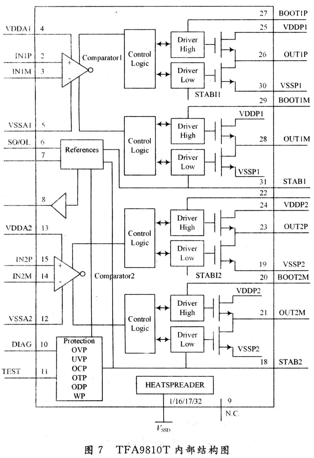
It has the following features: it can cancel the radiator, has high reliability, 8~20 V single power supply, external gain adjustable, standby power supply state of the micro-ampere level, low energy consumption. Ideal for tablet TV products, multimedia systems, and wireless audio.
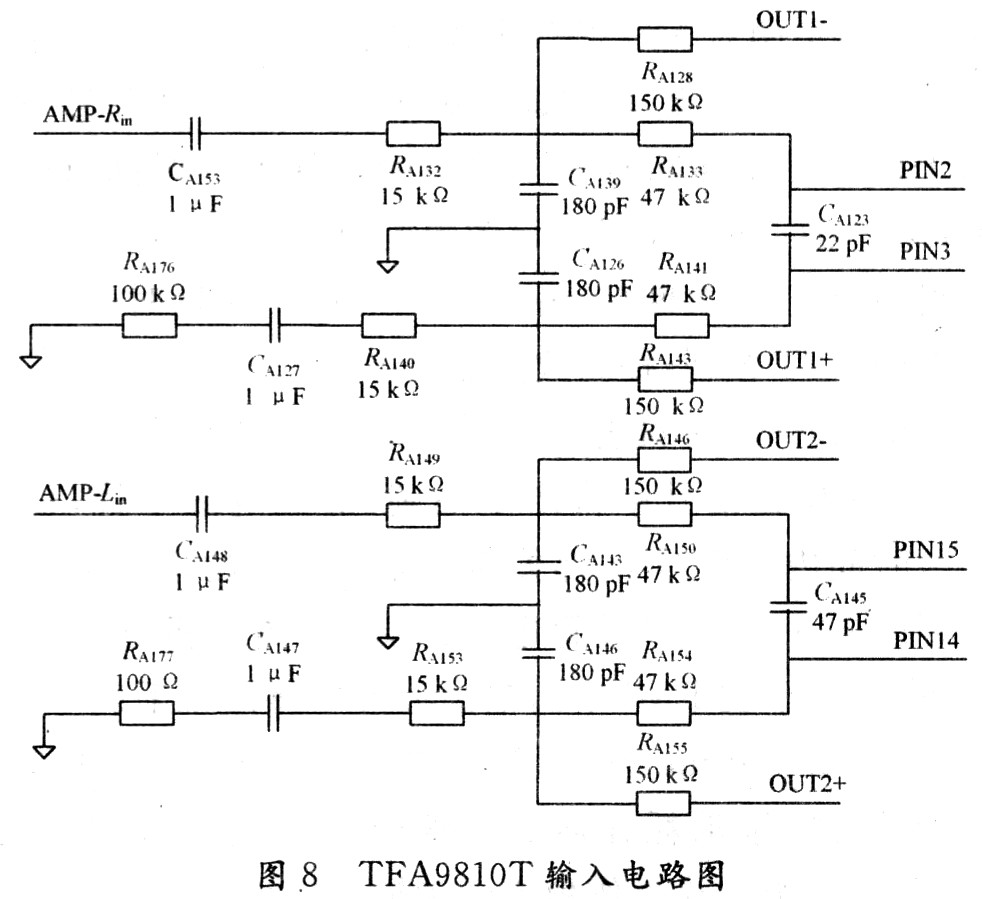
3.2 Analog Input Stage Design The TFA9810T input uses a fully differential input circuit that rejects common mode interference. Taking the AMP-Rin input of Figure 8 as an example, RA128/RA133/CA139 constitutes a negative feedback low-pass filter for attenuating the high-frequency carrier component of the feedback signal. Increase the amount of low frequency component feedback, especially the DC component. Effectively improve the duty cycle error caused by the difference between the input signal DC level and the comparator threshold voltage at zero input. Adjusting RA128 can also achieve TFA9810T gain control, so that Au(dB)=20log(VOUT/VIN)≌20log(RA128/ RA132). The internal resistors of the devices CA153/RA132/RA133 and TFA9810T form a high-pass filter for buffering the input signal. If the capacitance of CA153 is too small, it will affect the low frequency response. The theoretical formula is:
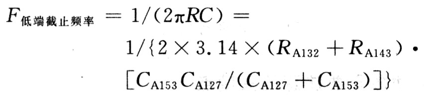
The design takes a value of 1 μF and determines that the low-end frequency is 16 Hz. If the frequency is set too high, the low-side input reactance (eg, at 20 Hz) will be too large, which may result in large noise and DC offset noise at the output ( Plop-noise). After the feedback signal is compared with the buffered input audio, the RA133 enters the TFA9810T for PWM modulation. In order to avoid the squeaking noise at the output end due to the nonlinearity of the Rin/Lin input signal in Fig. 8 due to the nonlinearity of the semiconductor, the two carriers are adjusted to a frequency of about 50 kHz by adjusting the capacitance CA123/CA145. In this design, CA123=22 pF and CA145=47 pF will be used to achieve a Rin/Lin carrier frequency difference of 50 kHz.
3.3 Output Stage LPF Low-Pass Filter Design The TFA9810T output low-pass filter uses a second-order Butterworth filter. The actual Butterworth second-order filter is from the RCA-type electronic component CA135/RA145/CA136 in Figure 9. /LA5/CA137/CA138/RA148/CA159/CA140/CA141/RA152/LA6/CA142/CA144, etc., which exhibits a straight-through effect on the 15 Hz to 20 kHz audio component in the PWM square wave, and above 20 kHz over the audio range The high frequency component exhibits a -12 dB/octave roll-off rate.
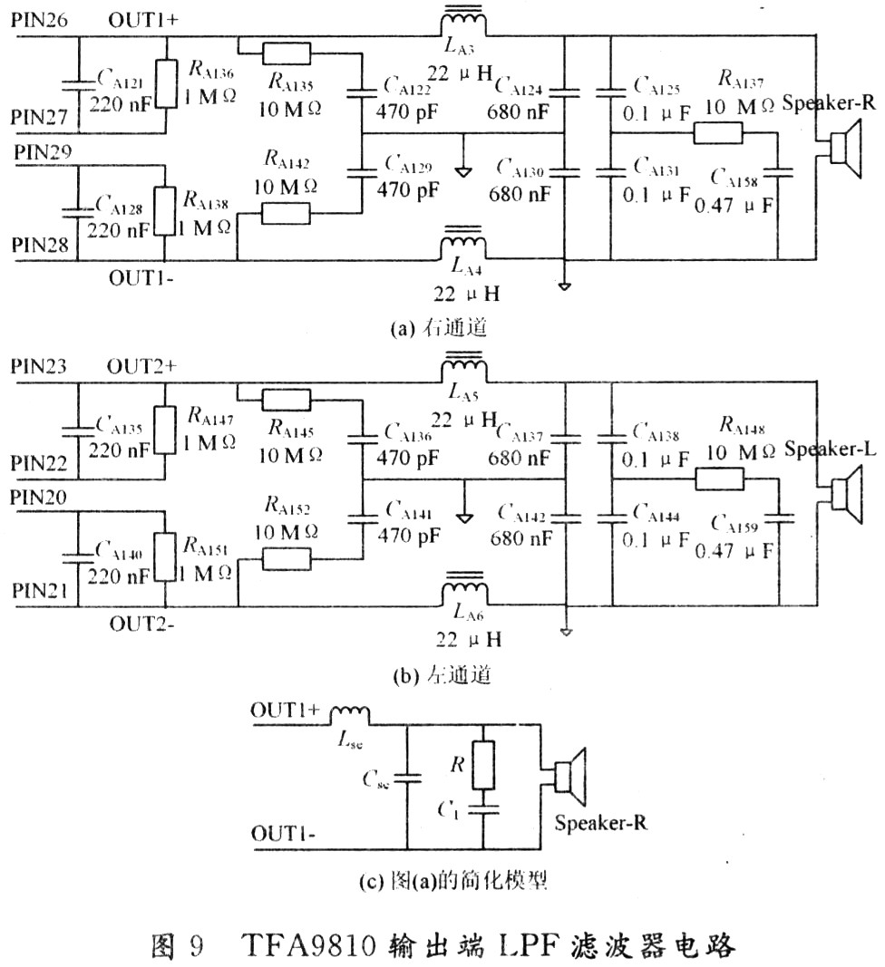
In the simplified model, Lse and Cse, R, C1 form the basic Butterworth filter, and R and C1 form a Zobel network peak-canceling circuit to remove spike interference at high frequencies.
3.4 Temperature rise test This design power amplifier TFA9810T DC power supply 15.2 V, working environment temperature is 20 ° C, audio system input is 2Vp unmodulated 1 kHz single audio signal, matching load is 8 Ω speaker, adjust audio output The power is 21 W, and it lasts for 30 min. Using the temperature test equipment, the maximum temperature of the TFA9810T housing is 45 °C, and the temperature rise is only 25 °C. There is no need to increase the heat sink.
3.5 Audio A/D/A Test Analysis Figure 10 tests the TFA9810T amplifier's audio input to 2 kHz at 1 kHz. Single audio signal waveform, the output speaker terminal to GND is 12.84V. , LPF in Figure 9. The PWM waveform output by the power amplifier before filtering. 11 to 13 respectively expand the A/B/C area in Fig. 10.
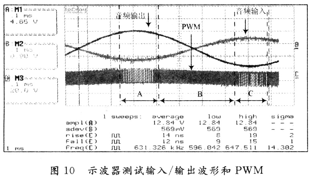
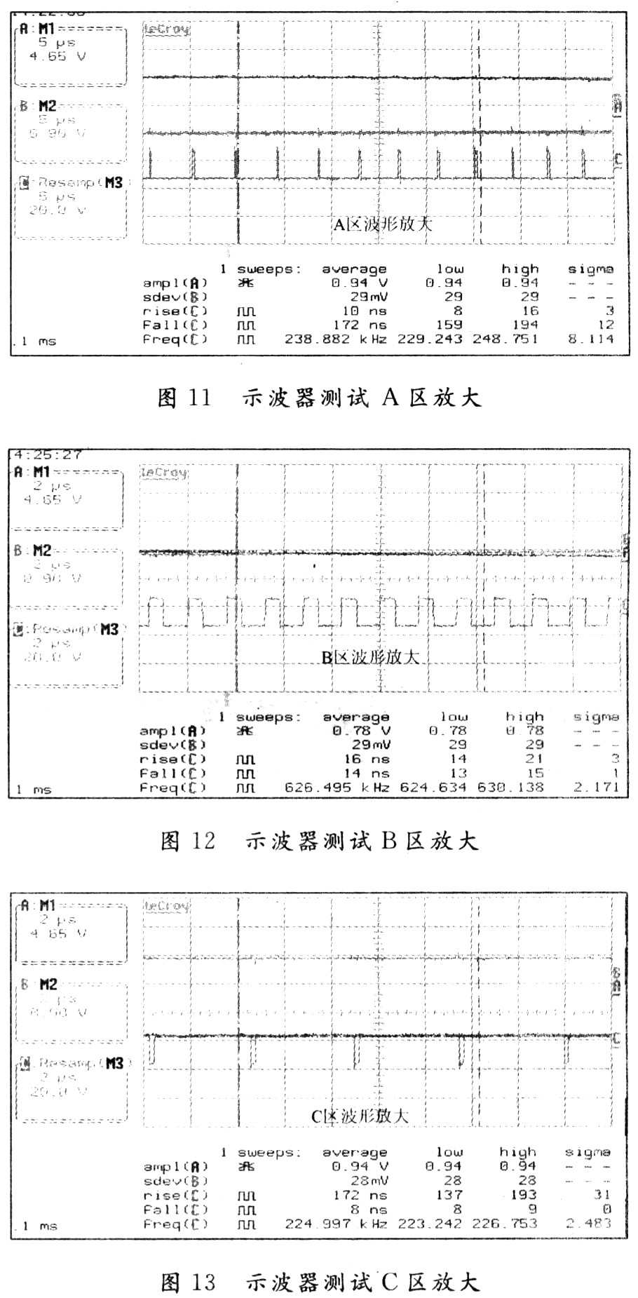
As can be seen from Figs. 10 to 13, the input waveform is superimposed with high frequency noise. The front end introduces bad interference, which needs further analysis and improvement; the output waveform is smooth, there is no crossover distortion, and the Deadtime characteristic is better; the input/output sine wave phase is opposite, and the closed loop negative feedback path is directly formed by the resistor RA128, which reduces noise interference, and Perform gain control. The extended graphs of the A, B, and C regions output the sinusoidal peaks, troughs, and PWMs at the S region at 238.8 kHz, 224.9 kHz, and 626.4 kHz, respectively, with different duty cycles, which are consistent with the triangular wave sampling characteristics. In the figure, the falling edge of the PWM pulse fall and the rising edge of the rise are steeper. Compared with the S-shaped region, it contains a lot of high-frequency harmonics, which easily cause EMI radiation, but is filtered by Butterworth second-order filter. The sine wave is good, no obvious high-frequency clutter is superimposed, and the EMC test has no obvious external radiation frequency, which satisfies the design needs.
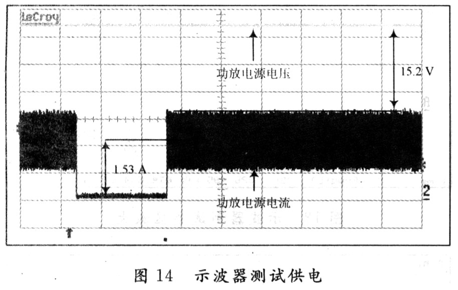
3.6 Power and Efficiency Test Figure 14 tests the actual waveform of the supply voltage and current of the power amplifier TFA9810T in the state of Figure 10.
As can be seen from Figure 10, the single-ended output power of the power amplifier is:
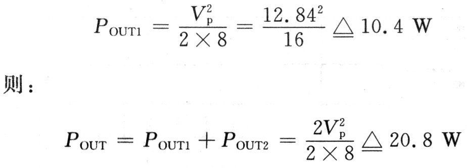
It can be seen from the parameters of Figure 14 that the total power carried by the power amplifier power supply system is: ![]()
The efficiency of the TFA9810T is thus:
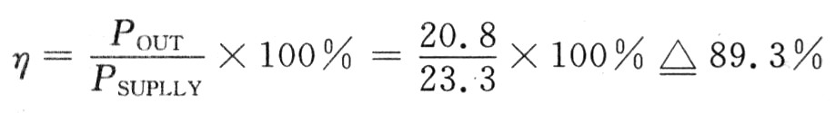
4 Conclusion This paper introduces the analog full-bridge D-class power amplifier topology structure, and discusses in detail the second-order Butterworth filter design and power amplifier PCB layout, which suppresses the EMI generated by Deadtime. Finally, based on NXP's Class D power amplifier TFA9810T, a new green energy efficient dual-channel Class D audio amplifier design was realized. Simulation and test results show that the amplifier can provide 10 W × 2 output power to two 8 Ω speakers at a supply voltage of approximately 15 V, with a conversion efficiency of 90%, total harmonic distortion of less than 7%, and 1 kHz sine wave audio. The output has no crossover distortion, no obvious EMI interference, and the relative temperature rise of the power amplifier housing is 25 °C. With the energy saving requirements of today's society, this kind of green energy efficiency design will reach a wider range of applications in the next few years.
Single USB Travel Plug,Industrial Wall Mounted Socket Outlet,Australian Usb Power Wall Socket
Double USB Travel Plug,Single Country Plug Adapter Co., Ltd. , http://www.chtravelplug.com