0 Preface
The SDI interface (Serial Digital Interface) directly controls the video signal by means of digitization. Processing and transmission, digital video or audio signals are transmitted through a single-core coaxial cable in an effective field, and then digital signals are directly connected to subsequent processing systems to avoid traditional analog signals due to A/D and D/A conversion bands. The resulting image detail and quality loss also make the interaction between devices easier and more convenient.
The SDI interface has a high transmission rate. Adaptable. Plug and play. Due to its low environmental requirements and wide range of applications, SDI has been used as a protocol standard for military imagery equipment in many strategic shooting ranges in China.
At present, in terms of civilian use, the SDI interface has been accepted and adopted by most video equipment manufacturers in the world as a standard video transmission interface, and is involved in the field of digital photography. Television movies and professional studios. World famous Sony. Video devices produced by companies such as Panasonic support the SDI interface protocol.
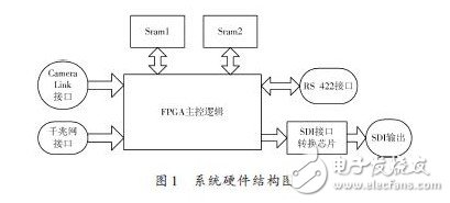
1 system hardware structure
The system structure is shown in Figure 1, mainly by the Camera Link interface. Gigabit network interface. Large-capacity SRAM memory, FPGA chip, SDI interface chip and SDI interface monitor. Here FPGA is the core logic of the whole system, using XILINX company's V2 series XC2V4000FFG1152 chip, the chip has 1 152 IO pins, 4 MB system gate unit, 120 multipliers, 12 digital clock managers, 824 users The block RAM of IO, 120 & TImes; 18 b can be defined. The rich hardware resources provide a reliable guarantee for the display and enhancement processing of the input image. The basic working process of the system first receives the image data of the Camera Link interface or the Gigabit network interface, and converts the data into TTL or CMOS format through a dedicated interface conversion chip, and transmits it to the FPGA, and performs real-time image processing inside the FPGA. The protocol converts and outputs the data conforming to the SDI interface chip, and the SDI standard definition image data is output in real time through the parallel conversion of the interface chip.
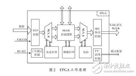
The main working principle of FPGA here is shown in Figure 2. In this module, after the system is powered on, the configuration of the SDI interface chip working register is completed first, thereby completing the selection of its working mode; then the input image data interface to the interface chip's line clock protocol conversion and data to the YCbCr format are completed. Conversion, here the FPGA uses double buffer control to complete the format conversion. This article applies frame scaling. Grayscale stretching and pseudo color processing implement image enhancement processing, which is described in detail in the next section.
2 image enhancement algorithm
2.1 Grayscale stretching algorithm
Nowadays, many cameras are based on CameraLink interface and Gigabit network interface. Their output data bits are 8 b, 10 b and 14 b. The system is intelligently processed in the system design, and the system is connected to the system through the RS232 serial port of the host computer. The conversion module sends a command signal to inform the system of the number of gray data bits and the number of data bits at the system output, so that the algorithm achieves different grayscale stretching. Since the general monitor can only display image data of 8 b gray scale, the SDI signal has two differences of 8 b and 10 b. To perform a linear stretch on the grayscale image, the algorithm can be used to map the image data to the 8b and 10b spaces, which is the stretching process described below, regardless of the number of bits of the front-end input image data. Here, taking the input image data 14 b as an example, assuming that the input is 10 b image data, the macroscopic concept is to linearly map the 14 b data space to the 10 b space. Assuming that the gray value before grayscale stretching is Yi, its gray value range is [0,16 383]; the gray value after gray stretching is Yi′, and its value range is [ 0,1 023], then the direct direct mapping relationship between Yi and Yi ′ is:
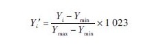
Where: Ymax is the maximum value of the gray of a certain frame image; Ymin is the minimum value of the gray of a certain frame image.
If the output is 8 b image data, the 14 b gray scale is converted to the 8 b gray space as needed, and the linear mapping relationship is:
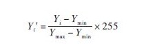
Where: Ymax is the maximum value of the gray of a certain frame image; Ymin is the minimum value of the gray of a certain frame image.
According to the above formula, it is necessary to use the basic multiplication and division operation when performing the stretching transformation. This is difficult to implement in the Xilinx FPGA. The most common method is to call the multiplication and division IP core inside the FPGA. Can greatly improve the efficiency of the FPGA. According to the above formula, if you want to implement the algorithm, you need to know the gray minimum and maximum value of the current frame image data. The FPGA work is clock-based and has real-time performance. If you want to get the gray value of the current frame, The image data needs to be cached and then the maximum value is extracted twice. In the program implementation, for the sake of simplicity, the maximum value and the minimum value of the current frame are used instead of the maximum value and the minimum value of the current frame. In this way, the current frame traversal is obtained to obtain the highest value, and then applied to the next frame image. Here, it is considered that the front and back frame correlation is relatively large, and the algorithm is not greatly affected.
2.2 pseudo color processing
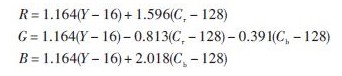
After the image data input by the black-and-white camera is processed by the protocol conversion, the luminance Y component of the SDI interface video YCbCr format is obtained. At this time, CbCr is filled in the program for 80 hours to form a YcbCr signal, and then used for output display, in order to enhance the display effect. The color is more enriching the visual effect of the human eye. An algorithm is given below to convert the grayscale into pseudo color.
To achieve pseudo color processing, the RGB pseudo color code table is usually searched by using the current pixel gray value as a storage address, and the corresponding RGB three color values ​​in the code table are converted into YcbCr color intervals by RGB, and then the pseudo color image is output. The basic method implemented in the FPGA is to make maximum use of the IP core of the FPGA, write the RGB code table to the embedded RAM core of the FPGA, traverse the lookup table in sequence and calculate the following formula to calculate the corresponding CbCr value. Output.
2.3 Frame Zoom
Image frame scaling is also known as image resampling, which is an important technique in video processing. In the SDI display output module, since the SD resolution of the SD SDI display is 720 & TImes; 576, the image resolution of the front-end input CameraLink or other interface is random, so the image frame scaling is inevitably used. Otherwise, if the image resolution exceeds SDI This range will result in incomplete display. If the resolution is less than this range, it will result in a black frame, which directly affects the subsequent display effect.
At present, there are many kinds of algorithms for frame scaling, but the basic methods are algorithms for interpolation operations, such as nearest neighbor interpolation. Bilinear interpolation and cubic convolution interpolation algorithm, etc., but the nearest neighbor interpolation algorithm is rough at the edge of the image with faster brightness change; the cubic convolution interpolation algorithm is very complicated and has a large amount of computation, which does not satisfy the real-time processing conditions. Compared with the previous two interpolation algorithms, the bilinear interpolation algorithm has less computational complexity. High real-time performance, suitable for implementation inside the FPGA.
As shown in Figure 3, assuming a point (x, y) in the original image, the adjacent right and lower pixel positions are (x + 1, y), (x, y + 1), (x + 1, y + 1), assuming that their gray values ​​are P1, P2, P3, P4, respectively, the displacement in both the horizontal and vertical directions is unity 1, and the position coordinates of the point to be inserted are assumed to be: (x + d ) x , y + dy .
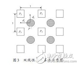
Then the gray value of the insertion point is obtained according to the principle of bilinear interpolation algorithm:
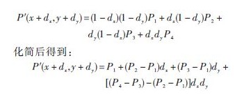
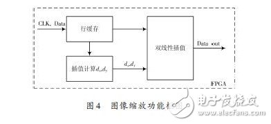
It can be seen from the above formula that when the offset distances dx and dy of the points to be interpolated are known, the gray value of the interpolated pixel points can be obtained according to the surrounding four points. The frame scaling process in this system uses the bilinear interpolation algorithm. The specific functions implemented in the FPGA are shown in block 4, mainly by the data buffer unit. Bilinear interpolation unit. The interpolation coefficient control unit is composed.
Before implementing the image scaling algorithm, the scaling factor k of the image is first calculated. Here, taking a line image as an example, the distance between adjacent pixels is represented by a unit length "1", and the resolution before image scaling is A & TImes; The scaled resolution is B &TImes; 1, then the pixel scaling factor k = BA for the image before and after scaling. For example, an image with a resolution of 640×512 is scaled to an image of 720×576, and the scaling factor k=1.25 in the horizontal direction; the scaling factor k=1.125 in the vertical direction; horizontally according to different situations. The scaling factors in the vertical direction are different.
According to Figure 4 and the interpolation formula, the interpolation coefficient dx, dy needs to be provided to the interpolation operation module in real time after one pixel clock. This requires FPGA timing synchronization, and the FPGA function modules can cooperate effectively.
China Bakery Pos Software,Best Pos For Bakery,Best Pos System For Bakery Supplier
Gmaii Bakery Pos System smart and easy-to-use POS for bakeries will turn your business into a thriving enterprise.
Gmaii Bakery Pos System being used in a bakery
Increase income
It all boils down to profit. Gmaii Bakery Pos Syste point of sale is designed to minimize transaction times and maximize your dollars per hour. "Next guest please!"
Never miss a sale
Gmaii Bakery Pos System keeps things running smoothly. While you focus on your happy customers, you can enjoy complete peace of mind.
Cakes and pastries on a window display
Diversify, track, grow
ShopKeep's detailed analytics track everything: from your bakery's raw ingredients, to sales trends, to your top-sellers. Fine-tune your menu with insightful data.
Don't miss a beat
If you need to duck out for an hour, or even take a day off, you can keep track of your bakery's sales in real time, from your desktop or smartphone. Life-changer.
Gmaii Bakery Pos System on a tabletop in a bakery
Versatile Gmaii Bakery Pos System: The Bliss Patisserie Way
Bliss Patisserie in Prairieville, LA used Gmaii Bakery Pos System to greatly decrease transaction times, grow profit margins, and maximize profits.
Bakery Pos System
Bakery Pos Software,Best Pos For Bakery,Best Pos System For Bakery,Pos System Dual Screen
Shenzhen Gmaii Technology Limited , https://www.gmaiipos.com