Switching power supplies have become a fundamental part of modern electronics, offering energy-efficient solutions for a wide range of applications. From computers and smartphones to automotive systems and industrial equipment, these power supplies are essential in delivering stable and efficient power. One of the most widely used topologies in consumer electronics is the DC-DC step-down (or buck) converter. These converters are especially popular due to their ability to efficiently reduce voltage while maintaining high current output.
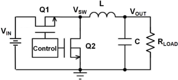
Figure 1: Synchronous buck converter circuit diagram.
A synchronous buck converter is designed to regulate voltage at a lower level than the input. It uses two power MOSFETs—typically referred to as the high-side (Q1) and low-side (Q2)—to control the flow of current through an inductor and capacitor. The key advantage of this design is that it reduces power loss by eliminating the need for a diode in the low-side switch, which is replaced by a second MOSFET. This results in better efficiency and less heat generation.
When Q1 is turned on, current flows from the input through the inductor to the load. During this time, Q2 is off, and the inductor stores energy. When Q1 turns off, Q2 turns on, allowing the stored energy in the inductor to continue supplying power to the load. This cycle repeats continuously, ensuring a steady output voltage. The switching node between the two MOSFETs is also smoothed by the LC filter, resulting in a stable DC output.
The duty cycle of the converter determines how long the high-side MOSFET remains on during each switching cycle. A higher duty cycle means more power is delivered to the load, while a lower duty cycle results in a reduced output voltage. For example, a 50% duty cycle would produce an output voltage roughly half of the input, while a 10% duty cycle would result in about 10% of the input voltage. Properly setting the duty cycle is crucial for achieving the desired output and maintaining system stability.
Power losses in a buck converter can come from multiple sources, including the MOSFETs themselves, the controller or driver, the feedback loop, and even the PCB layout. As technology advances, designers are pushing for higher switching frequencies, which allow for smaller components and improved efficiency. However, this also introduces challenges such as increased switching losses and electromagnetic interference (EMI).
The output stage of the converter, consisting of an inductor and a capacitor, plays a vital role in smoothing the output voltage and maintaining stability. The inductor stores energy during the on-time and releases it during the off-time, while the capacitor helps to filter out any remaining ripples. Selecting the right inductor and capacitor for a specific application is critical to achieving optimal performance.
Inductors vary in terms of material, inductance value, and DC resistance (DCR). A lower DCR is generally preferable because it reduces power loss and improves efficiency. However, there's a trade-off between inductance and ripple current. Lower inductance values lead to higher ripple currents, which can affect the stability of the output. Therefore, engineers must carefully balance these factors based on the application's requirements.
In summary, understanding the operation and design of a synchronous buck converter is essential for anyone working with power electronics. Whether you're designing a power supply for a smartphone, a server, or an electric vehicle, choosing the right components and optimizing the circuit configuration will ensure reliable and efficient performance.
LV Series(23.8"-98")
IR touch frame,open frame monitor,multi touch infrared touch frame,ir touch frame 32 inch,55 inch ir touch frame
Guangdong ZhiPing Touch Technology Co., Ltd. , https://www.zhipingtouch.com