Everyone is aware that impedance should remain continuous, but as Luo Yonghao once said, "There are always times when you step on the stool." In PCB design, it's common to encounter situations where impedance isn't perfectly continuous. So, how do we deal with this?
Characteristic impedance, also known as "characteristic impedance," is not a DC resistance but rather a concept used in high-frequency signal transmission along long lines. When a signal travels through a transmission line, an electric field is created, and this causes an instantaneous current to flow between the signal trace and the reference plane (such as ground or power). If the transmission line is uniform, the ratio of voltage to current during the signal’s travel creates an equivalent resistance, which is called the characteristic impedance, denoted as Z. Any change in this impedance along the path can cause signal reflections at the point of discontinuity. Several factors influence the characteristic impedance, including the dielectric constant, dielectric thickness, trace width, and copper thickness.
[1] Gradient Line
In some RF devices, the package size is small, and the SMD pad width may be as narrow as 12 mils, while the RF signal trace might be wider than 50 mils. To avoid abrupt changes in line width, a gradient line is often used. This transition line should not be too long to maintain signal integrity.
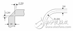
[2] Corner
If an RF signal trace makes a right-angle turn, the effective width at the corner increases, leading to an impedance mismatch and causing signal reflection. To minimize these issues, two common approaches are chamfering and rounding the corner. The radius of the arc should be large enough—typically R > 3W—to ensure smooth signal propagation.
[3] Large Pad
When a large pad is present on a 50-ohm microstrip line, it acts like a distributed capacitor, disrupting the continuity of the characteristic impedance. Two solutions are commonly applied: increasing the thickness of the microstrip medium and hollowing out the ground plane beneath the pad to reduce the parasitic capacitance. This helps maintain consistent impedance along the signal path.
[4] Via
A via is a plated metal cylinder connecting different layers of a PCB. Signal vias link transmission lines across layers, but they can introduce impedance discontinuities. A via stub refers to the unused portion of the via, while via pads are ring-shaped structures that connect the via to the top or internal layers. An isolation disk is an annular gap in power or ground planes to prevent short circuits.
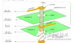
Parasitic Parameters of Vias
Through detailed physical analysis and approximation, the equivalent circuit model of a via includes a series of grounding capacitors at both ends of an inductor, as shown in Figure 1.
Passive Circuit Model
From the equivalent circuit model, a via itself has parasitic capacitance to ground. Assuming the reverse pad diameter is D2, the via pad diameter is D1, the board thickness is T, and the dielectric constant is ε, the parasitic capacitance of the via can be approximated as:
This parasitic capacitance can increase the signal rise time and slow down the transmission speed, degrading signal quality. Similarly, vias also have parasitic inductance. In high-speed digital PCBs, parasitic inductance is often more problematic than parasitic capacitance. Its series inductance reduces the effectiveness of bypass capacitors, weakening the filtering performance of the power system. The approximate formula for via inductance is given by:
Vias are a major source of impedance discontinuities in RF channels. For signals above 1 GHz, their impact must be considered. Common methods to reduce via-induced impedance discontinuities include using a diskless process, selecting an appropriate exit mode, and optimizing the anti-pad diameter. Optimizing the anti-pad diameter is one of the most widely used techniques. Since via characteristics depend on aperture size, pad dimensions, anti-pad size, stack-up structure, and exit mode, it's recommended to use tools like HFSS and OpTImetrics for optimization. Parametric modeling simplifies the process, and PCB designers should provide simulation documentation during reviews.
Changes in via diameter, pad diameter, depth, and anti-pad size can lead to impedance mismatches, resulting in reflection and increased insertion loss.
[5] Through-Hole Coaxial Connector
Similar to vias, through-hole coaxial connectors can also cause impedance discontinuities. Therefore, the same solutions apply. A common method to reduce impedance mismatch in these connectors is to use a diskless process, choose an appropriate exit mode, and optimize the anti-pad diameter. These adjustments help maintain signal integrity and reduce reflections in high-frequency applications.
Mitsubishi Diesel Generators :
·Engine and alternator shall be mounted on a same frame steel skid.
·Built-in damper for anti-vibration.·Small size, low weight, easy to operating, installation and maintenance.
·World most famous brand diesel engine: Mitsubishi Engine
·World famous brand AC alternator: Stamford, MeccAlte, Leroy Somer, etc
·Advanced and reliable controller: Auto Start AMF & Remote control by PC with RS232/485
·Full range protect function and alarm shutdown feature.
·Comply with ISO8528 national standard and ISO9001 quality standard.
Mitsubishi Diesel generator,Mitsubishi diesel genset,Mitsubishi genset,Mitsubishi generator,Mitsubishi diesel engine
Guangdong Superwatt Power Equipment Co., Ltd , https://www.swtgenset.com