introduction
High-voltage power supplies have been widely used in medical, industrial non-destructive testing, station, customs inspection and other testing equipment, and are also widely used in military fields such as radar transmitters and electronic aerial image displays. The traditional high-voltage Power Supply is bulky and cumbersome, which seriously affects the development of the supporting equipment. At present, the high-voltage power supply adopts the form of a switching power supply, which greatly reduces the volumetric weight, increases the power, and improves the efficiency. In particular, high-voltage small-power switching power supplies are almost all switching power supply structures. The high-voltage, low-power switching power supply discussed in this article is designed for the X-ray TV perspective system. This system is an improvement over the original X-ray equipment, which adds a device called an image intensifier. This device uses electrodes to accelerate and focus the electrons, thus requiring a low-power, high-voltage power supply that is compatible with it.
plan selection
The most common example of a low-power high-voltage power supply is the anode high-voltage generator of a television set. It converts a tens of volts of DC power through a power conversion and a high-voltage transformer, and then rectifies and filters it into a high-voltage output. Another application example is an anion. The generator is often thyristor regulated. Both of the above voltage regulation methods require a separately adjustable auxiliary power supply, that is, a combination of high and low voltage. This increases the size and complexity of the power supply. In addition, due to the different circuit structure forms, their output voltage range is limited, and when a large range of adjustment is required, it can only be achieved by changing the supply voltage. The main circuit voltage adjustment range of the X-ray enhancer is nearly 10kV, and the above circuit form is difficult to meet the requirements. The half-bridge resonant switching power supply used in this paper successfully solved the above problems.
Technical indicators
Input voltage 220 (1 ± 10%) V, (50 ± 0.5) Hz; or a wide range of input voltage 180 ~ 250V.
Output voltage / current
Anode (positive) voltage / current
Nominal value +25kV/1mA,
Voltage range +23kV ~ +32kV;
Nominal value +7.35kV/200μA,
Voltage range +6.0kV ~ +7.8kV;
Nominal value +0.985kV/200μA;
Voltage range +0.8kV to +1.1kV;
Cathode (negative) voltage/current
Nominal value -0.75kV/500μA;
Voltage range -0.5kV ~ -1kV.
The above four voltages are linked together.
Stability is 1%.
Operating temperature range 0 °C ~ +40 °C.
The storage temperature range is -40 ° C ~ +55 ° C.
Dimensions 160mm & TImes; 135mm & TImes; 43mm.
The electrodes of the image intensifier are inevitably burred during processing, and the tip discharge breaks the ignition at high voltage. To burn the burrs, a large current is required. In this way, on the one hand, the power output power is designed to be larger, and on the other hand, there should be perfect protection measures.
System block diagram and working principle
The system block diagram of the 25kV miniaturized high voltage power supply is shown in Figure 1.
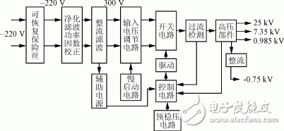
Figure 1 system block diagram
The input commercial power is purified and filtered, and then rectified into a DC voltage of about 300V and applied to the MOS tube of the half bridge circuit. The control circuit consists of the most commonly used SG3525 chip. The control circuit detects the amount of change of the output voltage through the feedback winding of the high voltage component, generates an excitation pulse to drive the power MOS FET, and realizes the regulated output. Technical difficulties and solutions
1, volume and insulation
This power supply is designed for X-ray intensifiers and is mounted in a small space under the X-ray intensifier base, requiring a small size. The reduction in volume is directly related to the choice of circuit form, the performance of the circuit, and the problems of insulation and heat dissipation. The circuit separates the power conversion, the control circuit and the like from the high voltage part, and selects the high-strength insulating medium to fill the high-voltage part, which solves the problem well.
2, high frequency and high voltage transformer
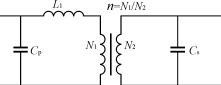
Figure 2 Transformer model considering distributed capacitance
The high frequency and high voltage transformer is the core component of the high voltage power supply. In a low-voltage (power) transformer, the distortion of the waveform and the problem of the operating band can be ignored, so that the influence of the distributed capacitance can be ignored. In high-frequency high-voltage transformers, due to the increase in the number of turns, especially the number of secondary turns, when the operating frequency of the transformer is relatively high and the rate of voltage change is relatively large, the distributed capacitance and leakage inductance must be considered. At this time, the transformer model is shown in Figure 2. L1 is the leakage inductance, and Cp and Cs are the distributed capacitances of the primary and secondary, respectively. The transformer leakage inductance L1 and the secondary distributed capacitance constitute a series resonant circuit. When the transformer is open or the load is light, the transformer can be regarded as an inductor, and thus forms a parallel resonant circuit with the secondary distributed capacitor Cs. The equivalent circuit is shown in FIG. When resonance occurs, the voltage across the capacitor will be higher than the operating voltage, which means that the voltage inside the transformer will be higher than the output voltage. This invisibly increases the withstand voltage requirements of the transformer. Therefore, in the winding process of the transformer, the distributed capacitance and leakage inductance should be minimized. Assuming that the capacitances of the layers are equal and the windings have a total of m layers, the distributed capacitance Cs=C (C is the secondary winding inherent capacitance and N2 is the secondary winding turns). When the number of secondary turns is constant, the distribution capacitance of the secondary equivalent to the primary is related to the number of layers of the secondary, and the more the number of layers, the smaller the distributed capacitance. The fewer the number of turns on each layer, the smaller the distributed capacitance. In order to reduce the distributed capacitance, a segmented group winding method is adopted, and the number of layers is increased to reduce the number of turns per layer. The transformer uses a horseshoe-shaped ferrite core, and its winding is schematically shown in Figure 4.
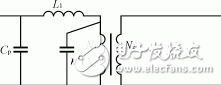
Figure 3 Distribution capacitor is equivalent to the primary equivalent circuit
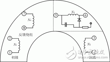
Figure 4 Schematic diagram of high voltage transformer winding
ZhenHuan`s line of wall mount External Battery Charger range in output power from 6 W to 40 W features high energy efficiency level VI and reliability, with quick charging function for 18650 batteries and li-ion batteries, etc. Our wall plug-in versions ac to dc power charger adopts constant voltage and constant current mode, all available with 2 colors LED indicator for charging status(Green and Red light). ZhenHuan`s power charger solutions include class II installations(without earth pin), equipped with US / EU / KR / UK / AU / CN AC plugs options.
6 Volt Battery Charger,On Board Battery Charger,Battery Charger Camera,Battery Charger LI Ion,External Battery Charger,Portable Battery Charger
Shenzhenshi Zhenhuan Electronic Co Ltd , https://www.szzhpower.com