Medical device system designers face many problems, including reducing the size, increasing functionality, and extending the life of implantable human device batteries, while ensuring safety through optimal safety, reliability, and efficacy. Designers must also consider the effects of single event turnover (SEU) caused by ionizing radiation from equipment used in radiotherapy environments, as this may lead to dangerous configuration changes.
Miniaturization has become a major growth driver for life-critical devices such as implantable cardioverter defibrillators (ICD) and heart rate management (CRM) products. One of the ways to reduce the size is to ensure that the radio frequency (RF) technology used to improve the functionality of medical devices consumes very low power, so smaller batteries can be used. Figure 1 shows the Pillcam wireless endoscopic imaging capsule from Given Imaging Ltd, which uses this technology. This product uses a custom RF transceiver from MGM, which can reduce the battery size by making the capsule power less than 7.5mW, and spreading up to 14 images per second during 8 hours of operation.
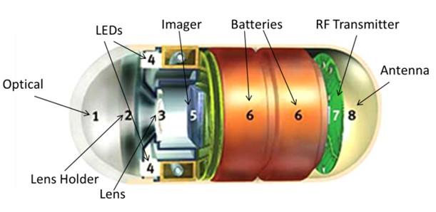
Figure 1: Pillcam wireless endoscope imaging capsule
The use of chip-on-board components, chip-on-chip, and recently advanced 2-D and 3-D packaging and other space-efficient semiconductor packaging technologies can also reduce device size. These packaging technologies can reduce the overall circuit space of heart rate management (CRM) devices by as much as 80%. One of the most effective techniques is the stacked-die method, which reduces interconnect length and resistance, while improving yield. Die stacking allows designers to combine multiple wafer processing technologies in a small volume while improving test access. The Thin Interconnected Package Stack (TIPS) project has made great progress in the next generation of stacked chip solutions. This project was invested by the nanoelectronics research organization IMEC R & D in cooperation with enterprises and social organizations. The TIPS project Provides a packaging method that reduces device height and other dimensions while having the advantages of a single module.
Field-programmable gate array (FPGA) devices are also important contributors to the miniaturization of equipment. For example, traditional designers have been using microcontrollers, dedicated standard product (ASSP) chips, and small programmable logic devices to build a portable medical device. Human Machine Interface (HMI) and micro motor controller. This method is not only difficult to reduce the size of the device, but also not suitable for optimizing the number of channels of vital sensors and actuators. On the contrary, FPGA-based solutions are very suitable for adding more functionality in a smaller package volume to meet the requirements of devices with small form factors. At the same time they provide additional advantages that allow users to upgrade their design, and thus can support new standards or provide more functionality.
Compared with alternative solutions, FPGA devices also help reduce power consumption. For example, the power consumed by liquid crystal display (LCD) panels in portable medical equipment accounts for half of the power budget of the application equipment. The solution is to design the system so that the LCD and control logic are placed in the power-saving mode as much as possible, greatly reducing battery consumption. This method of using FPGA is very simple, but because the design of spot ASSP products does not take into account the requirements of the medical market, it is difficult to use spot ASSP products to implement.
Today's FPGA devices based on flash technology also provide important built-in security features to ensure that only legitimate upgrades can be implemented, and other important security issues must be considered. Today's medical equipment is at risk of theft, counterfeiting, aftermarket tampering, and over-construction. Subcontractors have manufactured more equipment orders, so they can sell the remaining equipment. Each of these risks has serious consequences for the medical device market. Imagine the following scenario: the wrong software is downloaded to the insulin pump, or the fake parts are used in the design. Any situation may cause the insulin pump to provide an inaccurate dose, which will cause serious harm to the patient.
Protecting medical equipment from tampering requires inspections in both hardware and software, otherwise consumers may restore factory settings before making a claim, and there is no way to detect attacks. Computer hackers may modify the functionality of services and infrastructure to further hinder attack detection, response, and implementation of countermeasures.
The use of anti-fuse and flash-based FPGA devices is very important, because compared with SRAM-based FPGA, they are very difficult to reverse engineer. Once programmed, the flash-based FPGA retains all programming information in the chip. Since the programming unit is non-volatile, it can maintain state between power-up cycles. This is in contrast to SRAM-based FPGAs, which must reload configuration data at power-up to expose the programming bitstream to potential hackers. The only way for hackers to intercept the bitstream of a flash-based FPGA is to obtain it from the configuration file used to upgrade the field device. However, this can be prevented by encrypting in the FPGA device, and using flash memory to permanently store all encryption keys and settings.
Finally, the designer of the equipment used in the radiotherapy environment must ensure that the equipment is immune to dangerous SEU events, which can occur when high-energy particles or ions impact the NP junction dissipation zone. The charge from femtocoloumb to picocoloumb accumulates in this area, causing voltage and current transients. Using SRAM-based FPGA, the obtained linear energy transfer (LET) is sufficient to supply excessive energy to the NP junction and cause SEU events in the form of memory components (SRAM cells, registers, latches, or triggers) The status of the device) (bit flip).
For flash memory cells, the situation is very different. Flash is a non-volatile memory structure, including a floating gate between the control gate and the lower MOSFET structure, encapsulated in a good dielectric (see Figure 2), When the ion attacks or approaches the dissipation region of the flash cell, it still deposits charge. However, the critical charge amount (QCRIT) required for flipping the storage bit of the flash cell is much larger than that of the SRAM cell, and the flash cell used for configuration also has a very robust structure. Therefore, the flash unit used for FPGA configuration has SEU event immunity.
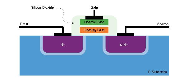
Figure 2: Flash memory unit
Miniaturization is becoming increasingly important for medical devices, and designers must provide better functionality, battery life, and safety, and this requires optimal safety, reliability, and efficacy. The latest FPGA technology combines ultra-low power chip design and advanced packaging technology to help significantly reduce device size. Compared with alternative methods, more functionality can be put into a smaller space while improving efficacy. Choosing flash-based FPGA technology can simultaneously reduce the risk of fatal security vulnerabilities and at the same time provide SEU immunity to equipment used in the radiation therapy environment.
Author: Senior Vice President of Microsemi's Communications and Medical Products (CMPG) / General Manager Stephen J. Swift
Telecom systems is the exchange of information over significant distances by electronic means. A complete, single telecommunications circuit consists of two stations, each equipped with a transmitter and a receiver. And we will offer the basic telecom products which you may familiar in your life to build up the telecom systems.
From Data center with a floor standing cabinets, you may get your sign out .For distribution outdoor, you may need a Waterproof Distribution Box to exchange the singals. Meanwhile, you may have a Terminal Block with 10 pair disconnection Krone Module and lighting protectors(LSA single pair type or STB Module ). When you distribute in house, there are more products in application like voice patch panels, keystone jacks, face plate, 3M connectors(like UY connectors), AMP picapond connector, wall outlets, surface mount box, and so on. Sure there is a must to get the right tool to finish operations, kinds of tools for selection: Insertion tools, Punch Tool , Crimping Tool , wire cutter, cable stripper. Hot sale for krone Insertion Tool , RJ45 crimping tools, Ericsson punch down tool, AMP picabond ratechet crimper, Coaxial Cable Crimping Tool .
We insist on compact size to ensure an easy but smart and reliable installation in every product of the telecom systems we offer. That is the final aim we work on solution, to make it perfect we also provide OEM service to satisfy your special demand. Till now, we have successfully take part in many Telecom projects in Russia, Sri Lanka, Greece, Ecuador, ect.. We have full experience in such tenders for building up telecom systems.
We keep on working just like the Cable Ring Managers to keep everything Orderly, Fast and Effective. Believe us and we will help you to be the winner !

Outdoor Distribution Box, LSA Krone Module, Mounting Frame, STB Module, Picabond Connector , Crimping Tool
NINGBO YULIANG TELECOM MUNICATIONS EQUIPMENT CO.,LTD. , https://www.yltelecom.com